Photovoltaic conversion element and method of manufacture thereof

A technology for photoelectric conversion components and manufacturing methods, which is applied in the fields of electrical components, semiconductor/solid-state device manufacturing, photovoltaic power generation, etc., can solve the problems of insufficient practicability, photoelectric conversion efficiency, insufficient durability, etc. Effect

Inactive Publication Date: 2014-07-16
JX NIPPON OIL & ENERGY CORP
View PDF12 Cites 8 Cited by
  • Summary
  • Abstract
  • Description
  • Claims
  • Application Information

AI Technical Summary

Problems solved by technology

However, only the durability under light irradiation for a relatively short period of about 20 hours was reported, and the practicality is insufficient.
As the use of ZnO, Cs 2 CO 3 For example, non-patent documents 4 and 5 report polymer-coated organic thin-film solar cells that combine polymer semiconductors (P3HT) and fullerene derivatives (PCBM), with insufficient photoelectric conversion efficiency and durability.

Method used


Image

  • Photovoltaic conversion element and method of manufacture thereof
  • Photovoltaic conversion element and method of manufacture thereof
  • Photovoltaic conversion element and method of manufacture thereof

Examples


Embodiment 1

[0116]

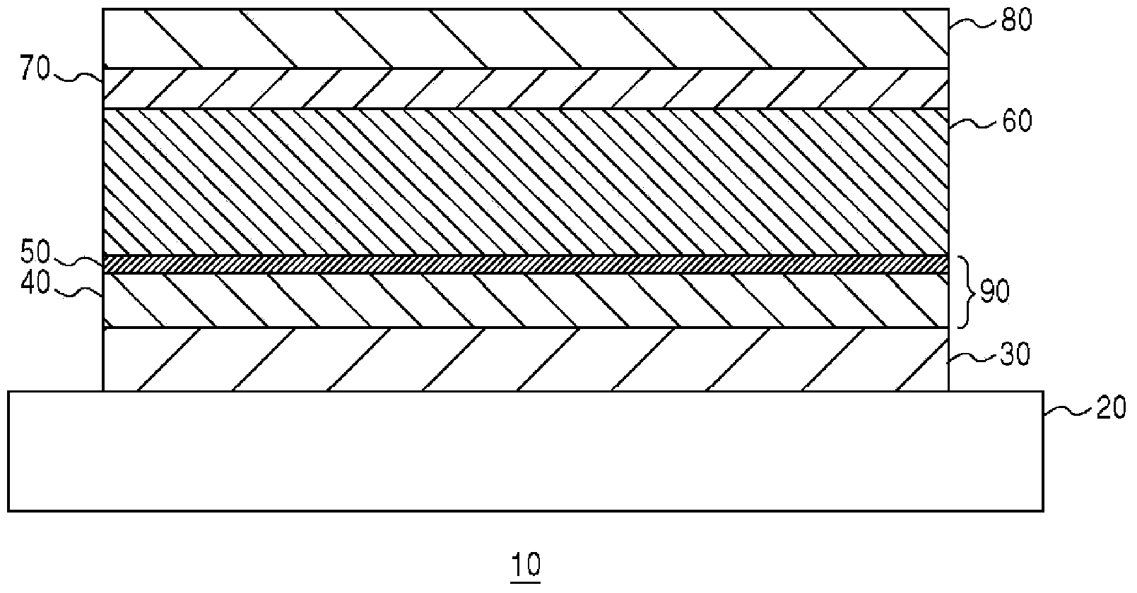
[0117] The glass substrate (surface resistance value 15Ω / □) obtained by forming a film of ITO by a sputtering method was washed to form an electrode for a negative electrode (electron output electrode).

[0118]

[0119] (1) Formation of electron transport layer

[0120] The electron transport layer was produced by the solution coating method. Specifically, zinc acetate dihydrate (manufactured by Aldrich) was dissolved in 2-methoxyethanol at a concentration of 20 mg / ml, and then monoethanolamine (55 μl / ml) was added to prepare a solution. The solution was spin-coated on the ITO for the negative electrode at 2000 rpm (30 seconds), and the heat treatment was performed on a hot plate at 120° C. for 5 minutes to form an electron transport layer (see Table 1). The thickness of the electron transport layer after the heat treatment was 30 nm.

[0121] (2) Formation of the energy regulation layer at the lower end of the conduction belt

[0122] Cesium carbonate (manufactured by Ald...

Embodiment 2

[0134] The manufacturing method of the photoelectric conversion element of Example 2 is the same as that of Example 1, except that the heat treatment temperature when forming the electron transport layer is 300°C. The manufacturing method of the photoelectric conversion element of Example 3 is the same as that of Example 1, except that ZnMgO is prepared as the electron transport layer as follows.

[0135]

[0136] Zinc acetate dihydrate (manufactured by Aldrich) and zinc acetate tetrahydrate (manufactured by Aldrich) were dissolved in 2-methoxyethanol at a concentration of 15mg / ml and 5mg / ml respectively, and then monoethanolamine (5.5μl / ml) was added. , Stir for 2 hours. The above-mentioned ITO for negative electrode was spin-coated with the above-mentioned solution at 2000 rpm (30 seconds) and heat-treated at 300°C for 5 minutes on a hot plate to form an electron transport layer. The thickness of the electron transport layer after the heat treatment was 30 nm.

Embodiment 4~6

[0138] The UV blocking film (manufactured by King Works Co., Ltd., KU-1000100, with a transmittance of 1% or less in the wavelength range of 370 nm or less) was pasted on the negative glass substrate, except that it was the same as Examples 1 to 3, respectively.


PUM

PropertyMeasurementUnit
thicknessaaaaaaaaaa
thicknessaaaaaaaaaa
transmittivityaaaaaaaaaa

Abstract

A photovoltaic conversion element (10) has a construction wherein an electron transport layer (40), a conduction zone bottom end energy adjustment layer (50), a photovoltaic conversion layer (60) and a positive hole transport layer (70) are sandwiched in this order between a first electrode (30) and a second electrode (80). The conduction zone bottom end energy adjustment layer (50) is formed by for example caesium carbonate. Also, the electron transport layer (40) is formed of zinc acetate.

Description

Technical field [0001] The present invention relates to a photoelectric conversion element that converts light energy into electrical energy through photoelectric conversion. Background technique [0002] Organic thin-film solar cells (photoelectric conversion elements) using organic semiconductors can use simple methods such as printing, light-weight and flexible materials such as plastic substrates, and roll to roll process (roll to roll process) such as large area, It is suitable for mass production and has the advantages of low cost, light weight, and flexibility compared with conventional solar cells. The expansion of the application range of solar cells can be expected. Therefore, the development of a new generation of solar cells is expected. At present, for the practical application of organic thin-film solar cells, progress has been made in the improvement of photoelectric conversion efficiency, and solar cells with a photoelectric conversion efficiency of more than 8% h...

Claims


Application Information

Patent Timeline
Patent Type & Authority Applications(China)
IPC IPC(8): H01L51/42C07C13/64C07C49/92
CPCB82Y10/00H10K85/113H10K85/215H10K30/30H10K30/50C07C13/64Y02E10/549C07C2604/00Y02P70/50H10K30/81H10K71/60
Inventor 市林拓朝野刚
Owner JX NIPPON OIL & ENERGY CORP
Why Eureka
Try Eureka