
Colored film substrate, manufacturing method thereof and display device

A technology of color film substrate and manufacturing method, which is applied in the field of flat panel display, can solve the problems of lower production yield, higher cost, alignment deviation, etc., and achieve the effects of improving product yield, reducing color shift, and improving quality

Inactive Publication Date: 2014-07-23
XIAMEN TIANMA MICRO ELECTRONICS +1
View PDF5 Cites 15 Cited by
  • Summary
  • Abstract
  • Description
  • Claims
  • Application Information

AI Technical Summary

Problems solved by technology

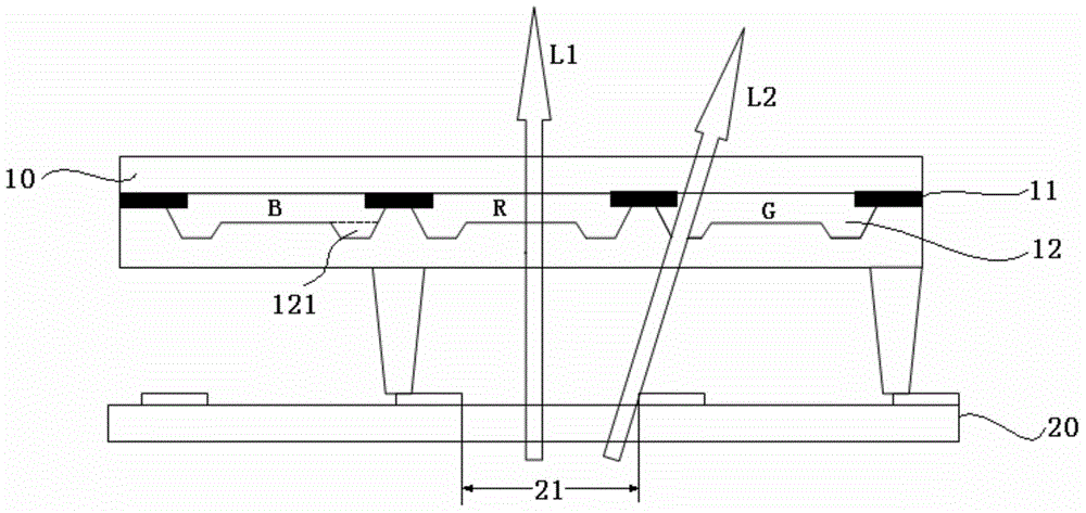
[0004] At present, in the manufacturing process of liquid crystal display devices, the color filter substrate and the array substrate 20 are bonded to form a liquid crystal display panel during the box forming process. Alignment deviation will occur, that is, the display area 21 of the pixel unit on the array substrate 20 cannot be accurately aligned with the color resist 12 on the color filter substrate
like figure 1 As shown, if the pixel unit is to display red, control the deflection of the liquid crystal molecules in the pixel unit area 21 corresponding to the red color resister R, so that light L1 passes through the red color resister R, but due to the alignment between the array substrate 20 and the color filter substrate Affected by the deviation, part of the light L2 will pass through the adjacent green color resistance G, especially when the display screen is observed at a large viewing angle, the color shift phenomenon will be particularly serious
In addition, since the color-resist layer 12 and the black matrix 11 have a partial overlapping area, the color-resist layer 12 produces bull-horn protrusions 121 in the overlapping area with the black matrix 11, which also makes the phenomenon of color mixing and color shift more likely to occur, resulting in Lower production yield and higher cost

Method used


Image

  • Colored film substrate, manufacturing method thereof and display device
  • Colored film substrate, manufacturing method thereof and display device
  • Colored film substrate, manufacturing method thereof and display device

Examples


Embodiment Construction

[0018] The following will clearly and completely describe the technical solutions in the embodiments of the present invention with reference to the accompanying drawings in the embodiments of the present invention. Obviously, the described embodiments are only some, not all, embodiments of the present invention. Based on the embodiments of the present invention, all other embodiments obtained by persons of ordinary skill in the art without creative efforts fall within the protection scope of the present invention.

[0019] An embodiment of the present invention provides a color filter substrate, such as figure 2 As shown, the color filter substrate includes a substrate 10, and a color-resist layer 11 directly arranged on the substrate 10. The color-resist layer 11 includes color-resistors of different colors. The red color resistance R, the green color resistance G and the blue color resistance B are directly arranged on the black matrix 12 on the color resistance layer 11, a...


PUM

PropertyMeasurementUnit
widthaaaaaaaaaa

Abstract

The invention discloses a colored film substrate. The colored film substrate comprises a substrate body, a color resistor layer and black matrixes, wherein the color resistor layer is directly arranged on the substrate body and comprises color resistors of different colors, and the black matrixes are directly arranged on the color resistor layer and arranged between every two adjacent color resistors. Due to the fact that the color resistor layer is directly formed on the substrate body and then the black matrixes are arranged on the color resistor layer, the perpendicular distance between the black matrixes and an array substrate is shortened, when light reaches the colored film substrate, unexpected emergent light is shielded through the black matrixes, the color cast phenomenon is reduced, the quality of displayed pictures is improved, and the yield of products is increased.

Description

technical field [0001] The invention relates to flat panel display technology, in particular to a color filter substrate, a manufacturing method thereof, and a display device. Background technique [0002] Liquid crystal display devices have the advantages of thinness, low power consumption and low radiation, and are widely used in various fields. The color filter film (hereinafter referred to as "color film") is a key component that can make the liquid crystal display device colorful, and present a bright, lifelike, vivid picture, and increase the value of its accessories. [0003] Color filter substrates in the prior art such as figure 1 As shown, it includes a glass substrate 10, a black matrix 11 formed on the glass substrate 10, a color-resist layer 12 formed on the black matrix 11, including a red color-resist R, a blue color-resist B, and a green color-resist G, and the backlight unit provides After the light passes through the color resists of different colors, the...

Claims


Application Information

Patent Timeline
Patent Type & Authority Applications(China)
IPC IPC(8): G02F1/1335
Inventor 李静吴玲沈柏平
Owner XIAMEN TIANMA MICRO ELECTRONICS
Learn More