Fringe-field-switching-type liquid crystal display device, array substrate and manufacturing method of array substrate

A liquid crystal display device and array substrate technology, which is applied to instruments, nonlinear optics, optics, etc., can solve the problems of large load of data line 11, large electric field difference, large power consumption, etc., so as to reduce signal transmission delay, The effect of reducing parasitic capacitance and improving quality

Inactive Publication Date: 2014-07-23
SHANGHAI AVIC OPTOELECTRONICS +1
View PDF9 Cites 39 Cited by
  • Summary
  • Abstract
  • Description
  • Claims
  • Application Information

AI Technical Summary

Problems solved by technology

For the FFS liquid crystal display device with high-resolution point inversion, the electric field difference between the pixel electrodes 16 of adjacent pixel regions 13 is relatively large, thereby forming a large pixel electrode capacitance Cpp, which affects the display quality
At the same time, there is only an insulating layer between th

Method used


Image

  • Fringe-field-switching-type liquid crystal display device, array substrate and manufacturing method of array substrate
  • Fringe-field-switching-type liquid crystal display device, array substrate and manufacturing method of array substrate
  • Fringe-field-switching-type liquid crystal display device, array substrate and manufacturing method of array substrate

Examples


Embodiment 1

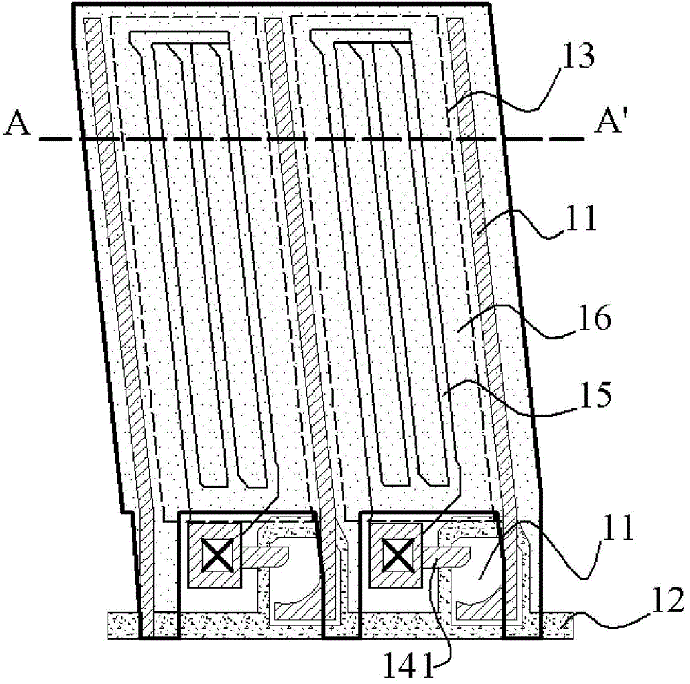
[0020] image 3 It is a schematic structural diagram of an array substrate of an FFS liquid crystal display device according to an embodiment of the present invention. Figure 4 for image 3 Sectional view along section B-B'. combine image 3 and Figure 4 As shown, the array substrate 2 of the fringe field liquid crystal display device includes a plurality of scanning lines 21, a plurality of data lines 22 formed by the first conductive layer, and the data lines 22 and the scanning lines 21 are arranged to cross each other to define a pixel area 23, usually , the first conductive layer may be aluminum (Al), titanium (Ti) or composite materials thereof. A gate insulating layer 211 is disposed on the substrate 20, and a data line 22 is disposed on the gate insulating layer 211. The data line 22 is covered with a first insulating layer 221. The first insulating layer may be made of silicon oxide or silicon nitride. The first common electrode 24 formed by the second conducti...

Embodiment 2

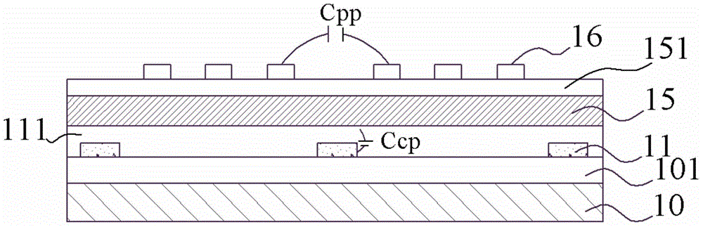
[0028] Figure 6 It is a structural schematic diagram of an FFS liquid crystal display device according to another embodiment of the present invention. Figure 7 for Figure 6 Sectional view along section B-B'. combine Figure 6 and Figure 7 As shown, the array substrate 2 of the fringe field liquid crystal display device of this embodiment includes a plurality of scanning lines 21, a plurality of data lines 22 formed by the first conductive layer, and the data lines 22 and the scanning lines 21 are arranged to cross each other to define pixels The area 23 covers the first insulating layer 221 on the data line 22, the first common electrode 24 formed by the second conductive layer is disposed on the first insulating layer 241, and covers the second insulating layer 241 on the first common electrode 24, The second common electrode 25 and the pixel electrode 26 formed by the third conductive layer are formed on the second insulating layer 241 , and the pixel electrode 26 is...

Embodiment 3

[0034] The manufacturing process of the array substrate of the FFS liquid crystal display device in the above embodiment will be described in detail.

[0035] First, if Figure 8a As shown, a substrate 20 is provided, and the substrate 20 may be a transparent glass substrate, and a gate metal layer (not shown in the figure) is sputtered on the substrate 20 . Aluminum (Al) can be used for the gate metal layer. Copper (Gu), chromium (Gr), molybdenum (Mo) or their composite materials. Patterning the gate metal layer, developing, exposing, and etching the gate metal layer to form gates and scanning lines (not shown in the figure), and covering the gates and scanning lines with a layer of gate insulating layer 211 .

[0036] Next, if Figure 8b As shown, the first conductive layer is sputtered on the gate insulating layer 211 , developed, exposed, and etched to form a plurality of data lines 22 and source and drain electrodes of the thin film transistor (not shown in the figure)...


PUM

PropertyMeasurementUnit
Widthaaaaaaaaaa
Widthaaaaaaaaaa

Abstract

The invention discloses an array substrate of a fringe-field-switching-type crystal display device. The array substrate comprises a plurality of data lines, a plurality of grid lines, pixel electrodes, first public electrodes and second public electrodes, wherein the grid lines and the data lines are arranged in a crossed mode to define pixel regions, the pixel electrodes are arranged in the pixel regions, the first public electrodes are formed between the data lines and the pixel electrodes, the positions, corresponding to the data lines, of the first public electrodes are hollowed out, the second public electrodes and the pixel electrodes are located on the same layer and the second public electrodes are overlapped with the data lines. According to the array substrate, stray capacitance between the first public electrodes and the data lines is reduced, signal transmission delay is shortened, and power consumption is lowered. Meanwhile, due to the arrangement of the second public electrodes, interference brought to the pixel electrodes by the data lines is shielded, stray capacitance of the pixel electrodes between the adjacent pixel regions is also reduced, interference of the pixel electrodes between the adjacent pixel regions is effectively absorbed, and the quality of displayed frames is improved.

Description

technical field [0001] The invention relates to flat panel display technology, in particular to a fringe field liquid crystal display device, an array substrate and a manufacturing method thereof. Background technique [0002] A fringe field (FFS, Fringe Field Switching) liquid crystal display device has the advantages of wide viewing angle, high aperture ratio, low power consumption, and high brightness, and is widely used in various fields. The FFS liquid crystal display device generates a fringe electric field through the electrodes between pixels in the same plane, so that the aligned liquid crystal molecules between the electrodes and directly above the electrodes can be rotated and switched in the plane direction parallel to the substrate, thereby improving the light transmission efficiency of the liquid crystal layer. The FFS liquid crystal display device overcomes the problem of low light transmission efficiency of conventional in-plane switching (IPS, In-Plane-Switc...

Claims


Application Information

Patent Timeline
IPC IPC(8): G02F1/1343G02F1/1333
Inventor 席克瑞曹兆铿崔婷婷
Owner SHANGHAI AVIC OPTOELECTRONICS
Why Eureka
Try Eureka