

Organic light-emitting display and its pixel circuit, driving method of the pixel circuit
A light-emitting display and pixel circuit technology, which is applied to circuits, static indicators, instruments, etc., can solve the problems of low integration of pixel circuits and uneven light emission of organic light-emitting displays, so as to increase the number of pixels, eliminate uneven light emission, reduce The effect of power loss
- Summary
- Abstract
- Description
- Claims
- Application Information
AI Technical Summary
Problems solved by technology
Method used
Image

Examples
Embodiment 1
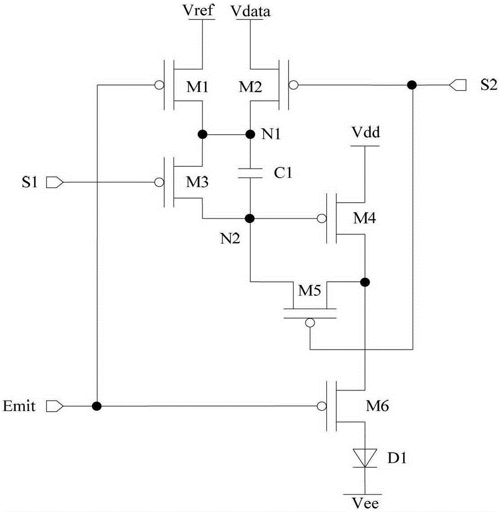
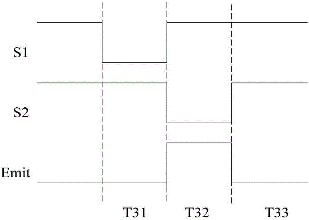
[0044] figure 2 is the driving signal timing diagram of the pixel circuit according to Embodiment 1 of the present invention, wherein the gate of the third transistor M3 receives the first scan signal S1, the gate of the second transistor M2 and the gate of the fifth transistor M5 The gate receives the second scanning signal S2, and the gates of the first transistor M1 and the sixth transistor M6 receive the control signal Emit.
[0045] refer to figure 1 with figure 2 , in the initialization phase T31, a control signal Emit with a first voltage amplitude is applied to the gate of the first transistor M1 and the gate of the sixth transistor M6, and the control signal Emit with a first voltage amplitude Turning on the first transistor M1 and the sixth transistor M6; applying a first scan signal S1 with a first voltage amplitude to the gate of the third transistor M3, and the first scan signal S1 with a first voltage amplitude The first scanning signal S1 turns on the third...
Embodiment 2
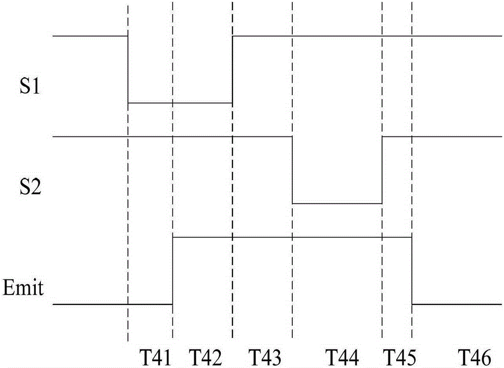
[0059] image 3 It is a timing diagram of driving signals of the pixel circuit in Embodiment 2 of the present invention. The signals applied to the pixel circuit in the initialization phase T41, the data writing phase T44 and the light emitting phase T46 are similar to those in Embodiment 1, and will not be repeated here. In the following, only the transitional stages between the above three stages will be described.
[0060] refer to image 3 , during the first time period T42 between the initialization phase T41 and the data writing phase T44, applying the control signal Emit with the second voltage amplitude to the gate of the first transistor M1 and the The gate of the sixth transistor M6 is used to cut off the first transistor M1 and the sixth transistor M6; the first scanning signal S1 with the first voltage amplitude is applied to the gate of the third transistor M3, Turning on the third transistor M3; applying the second scan signal S2 with the second voltage amplitu...
Embodiment 3
[0067] Figure 4 It is a timing diagram of driving signals of the pixel circuit in Embodiment 3 of the present invention. The signals applied to the pixel circuit in the initialization phase T51, the data writing phase T54 and the light emitting phase T56 are similar to those in Embodiment 1, and will not be repeated here. In the following, only the transitional stages between the above three stages will be described.
[0068] refer to Figure 4 , during the fourth time period T52 between the initialization phase T51 and the data writing phase T54, applying the control signal Emit with the first voltage amplitude to the gate of the first transistor M1 and the The gate of the sixth transistor M6 turns on the first transistor M1 and the sixth transistor M6; applying the first scanning signal S1 with the second voltage amplitude to the gate of the third transistor M3 , turning off the third transistor M3; applying the second scanning signal S2 with the second voltage amplitude ...
PUM
 Abstract
Description
Claims
Application Information