Panel drive circuit and panel drive method

A panel drive circuit and drive transistor technology, applied to static indicators, instruments, etc., can solve the problems of uneven OLED drive current, reduced lifespan, and low yield rate of AMOLED backplane, so as to prolong the service life and display picture quality, Effect of reducing drive power consumption

Active Publication Date: 2014-07-30
TCL CHINA STAR OPTOELECTRONICS TECH CO LTD
View PDF8 Cites 18 Cited by
  • Summary
  • Abstract
  • Description
  • Claims
  • Application Information

AI Technical Summary

Problems solved by technology

[0006] At present, due to the immaturity of LTPS technology, the threshold voltage Vth uniformity of the TFT manufactured by LTPS technology is very poor, and there is drift, which leads to the unevenness of the driving current flowing through the OLED, thereby reducing the uniformity of AMOLED brightness.
Since AMOLED is driven by current, the brightness of OLED is determined by the magnitude of the current. The higher the current, the higher the brightness. However, if it is always in high brightness working mode, its lifespan will be greatly reduced.
In addition, the yield rate of AMOLED backplane is still very low, and the lifespan and color stability of OLED light-emitting materials are not ideal. Therefore, the mass production of AMOLED is not yet high enough.

Method used


Image

  • Panel drive circuit and panel drive method
  • Panel drive circuit and panel drive method
  • Panel drive circuit and panel drive method

Examples


Embodiment Construction

[0028] In order to further illustrate the technical means adopted by the present invention and its effects, the following describes in detail in conjunction with preferred embodiments of the present invention and accompanying drawings.

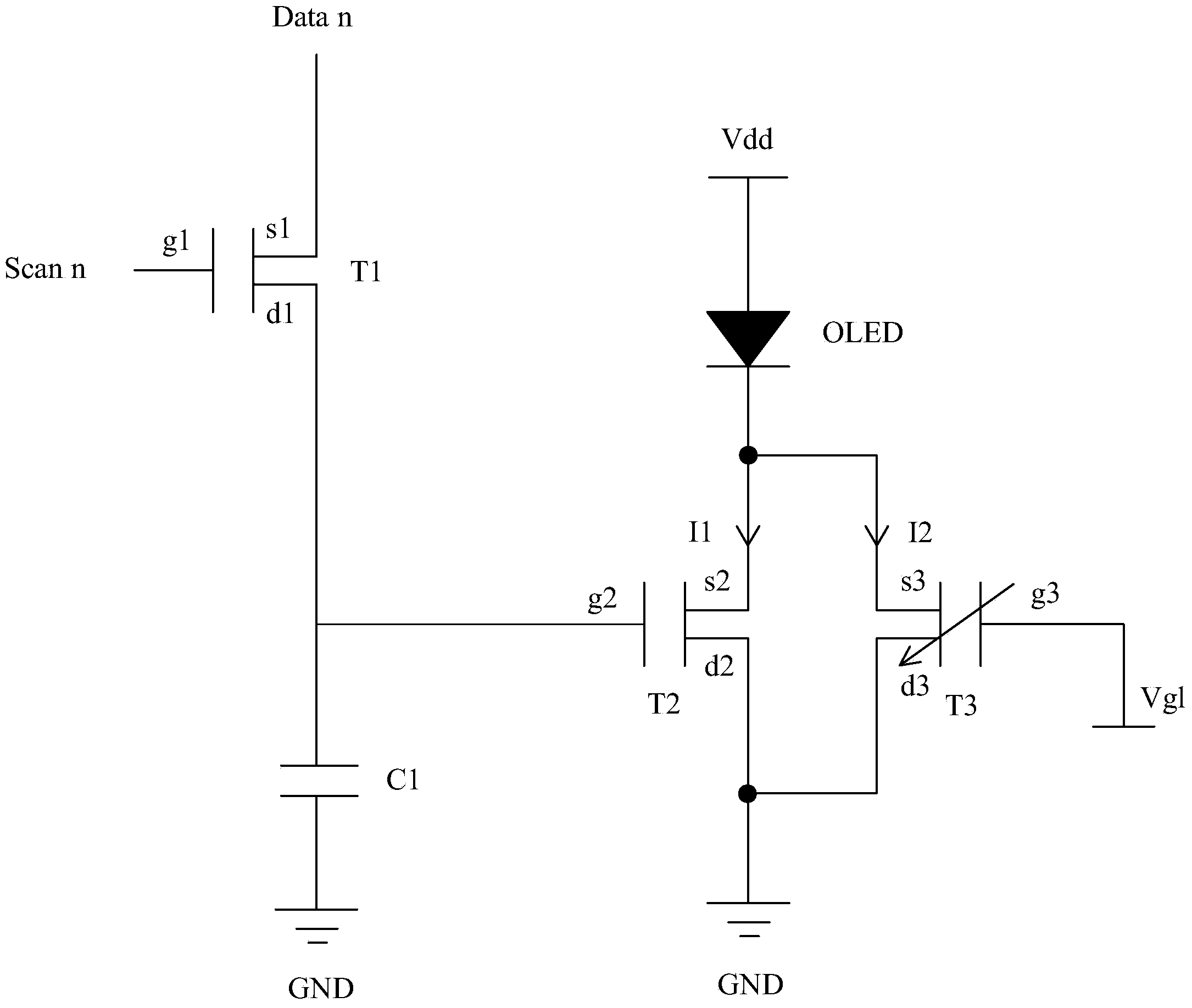
[0029] see figure 2 , figure 2It is a schematic diagram of a panel driving circuit of the present invention, including: a scanning control transistor (T1), a driving transistor (T2), a photosensitive transistor (T3), a storage capacitor (C1), and an organic light-emitting diode (OLED); and a scanning control terminal ( Scan n), a data signal terminal (Data n), a power supply voltage input terminal (Vdd), and a low voltage input terminal (Vgl); the scanning control transistor (T1) includes a first gate (g1), a first source (s1), and the first drain (d1), the drive transistor (T2) includes a second gate (g2), a second source (s2), and a second drain (d2); the photosensitive transistor (T3) includes a third gate (g3), a third source (s3), and...


PUM


Abstract

The invention provides a panel drive circuit and a panel drive method. The panel drive circuit comprises a scanning control transistor (T1), a drive transistor (T2), a photo-transistor (T3), a storage capacitor (C1) and an OLED. The panel drive circuit further comprises a scan control end (Scan n), a data signal end (Data n), a power voltage input end (Vdd) and a low voltage input end (Vgl). The drive currents of the drive transistor (T2) are gray-scale currents (I1), the currents of the photo-transistor (T3) are environment lighting currents (I2), the gray-scale currents (I1) depend on gray-scale voltages stored in the storage capacitor (C1), and the environment lighting currents (I2) depend on environment lighting. The luminance of a panel depends on the sum of the gray-scale currents (I1) and the environment lighting currents (I2).

Description

technical field [0001] The invention relates to the field of display technology, in particular to a panel driving circuit and a panel driving method. Background technique [0002] As a new generation of display technology, AMOLED (Active Matrix / Organic Light Emitting Diode, active matrix organic light emitting diode panel) has the advantages of high brightness, wide color gamut, wide viewing angle, fast response, and small size. Generally, an AMOLED driving circuit is manufactured using LTPS (Low Temperature Poly-silicon, low temperature polysilicon) technology. The light-emitting device of the AMOLED is an OLED (Organic Light-Emitting Diode, organic light-emitting diode). Driven by the AMOLED driving circuit, when a current flows through the light-emitting device OLED, the OLED emits light. [0003] At present, the AMOLED drive circuit usually adopts the traditional 2T1C circuit, please refer to figure 1 , is a traditional AMOLED panel drive circuit 2T1C. Including: scan...

Claims


Application Information

Patent Timeline
Patent Type & Authority Applications(China)
IPC IPC(8): G09G3/32G09G3/3233G09G3/3266
CPCG09G3/3233G09G2320/0233G09G2320/043G09G2320/0626G09G2330/021G09G3/3291G09G2300/0809G09G2300/0842G09G2360/144G09G3/3258G09G3/3266G09G2320/0646
Inventor 徐向阳
Owner TCL CHINA STAR OPTOELECTRONICS TECH CO LTD
Why Eureka
Try Eureka