Array structure fabric surface and preparing method and application thereof

An array-structured, textured technology for end-product manufacturing, chemical instruments and methods, sustainable manufacturing/processing, etc.

Active Publication Date: 2014-07-30
NINGBO INST OF MATERIALS TECH & ENG CHINESE ACADEMY OF SCI
View PDF8 Cites 17 Cited by
  • Summary
  • Abstract
  • Description
  • Claims
  • Application Information

AI Technical Summary

Problems solved by technology

[0004] In summary, there is still a lack of satisfactory, high-precision and high-etching rate, and mass-produced light-trapping technology (i.e. t...

Method used


Image

  • Array structure fabric surface and preparing method and application thereof
  • Array structure fabric surface and preparing method and application thereof
  • Array structure fabric surface and preparing method and application thereof

Examples


preparation example Construction

[0087] Preparation method of cone array textured surface

[0088] The present invention also provides a method for preparing the textured surface of the column array structure and the textured surface of the cone array structure of the present invention. Generally, a method for preparing a textured surface of a pillar array structure includes:

[0089] (a) providing a semiconductor substrate;

[0090] (b) laying a layer of polymer microsphere monolayer film on at least one main surface of the substrate, and etching the polymer microspheres in the monolayer film to form an etched The substrate of the etched polymer microsphere monolayer film;

[0091] (c) performing metal coating treatment on the substrate obtained in the previous step, thereby forming a metal thin film layer covering the upper surface of the etched polymer microspheres and covering at least part of the main surface of the substrate, so that The metal thin film layer contains a catalytic component for metal ...

Embodiment

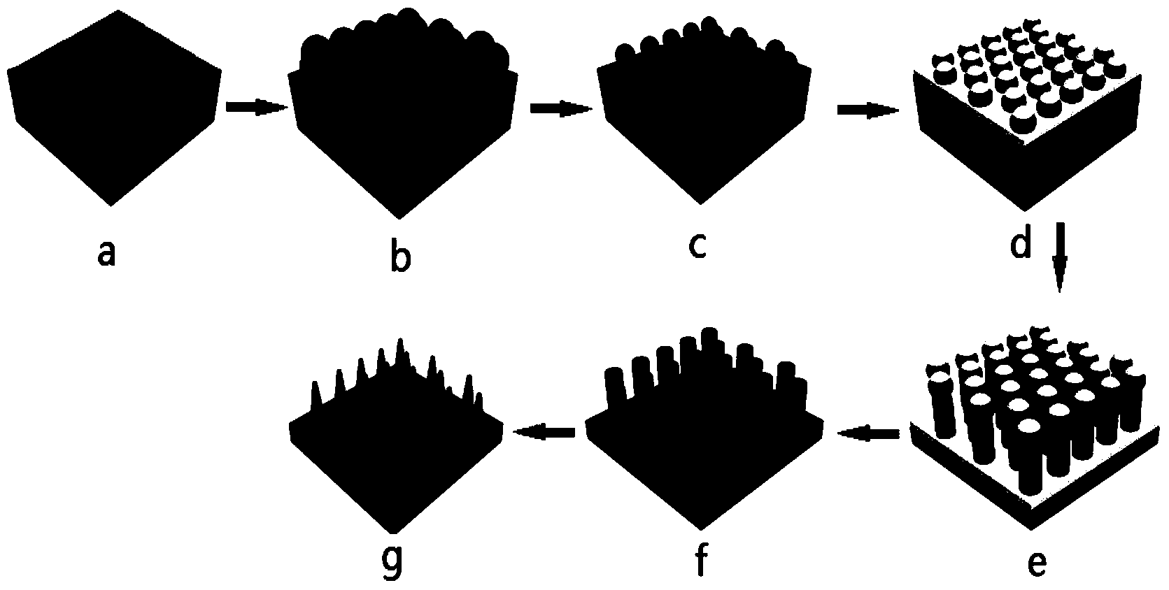
[0118] Preparation process description

[0119] figure 1 It is the basic flow chart of the specific preparation of the pile array joint pile surface and the cone array structure pile surface in the present invention. like figure 1 As shown, the preparation process is as follows:

[0120] (1) The substrate is cleaned and ready for use, such as figure 1 a shown in .

[0121] (2) Using the drift method in the self-assembly technology to form the polymer nanosphere array, and then laying it on the substrate, the size of the polymer nanosphere can be selected from 50nm to 1000nm, such as figure 1 b shown.

[0122] (3) After the polymer nanosphere array is etched by the reactive ion etching system (RIE), the array period remains unchanged, and the diameter of the nanosphere particles in the array can be selectively regulated, such as figure 1 c shown.

[0123] (4) Using methods such as thermal evaporation, electron beam evaporation or sputtering figure 1 The surface of the s...

preparation Embodiment 1

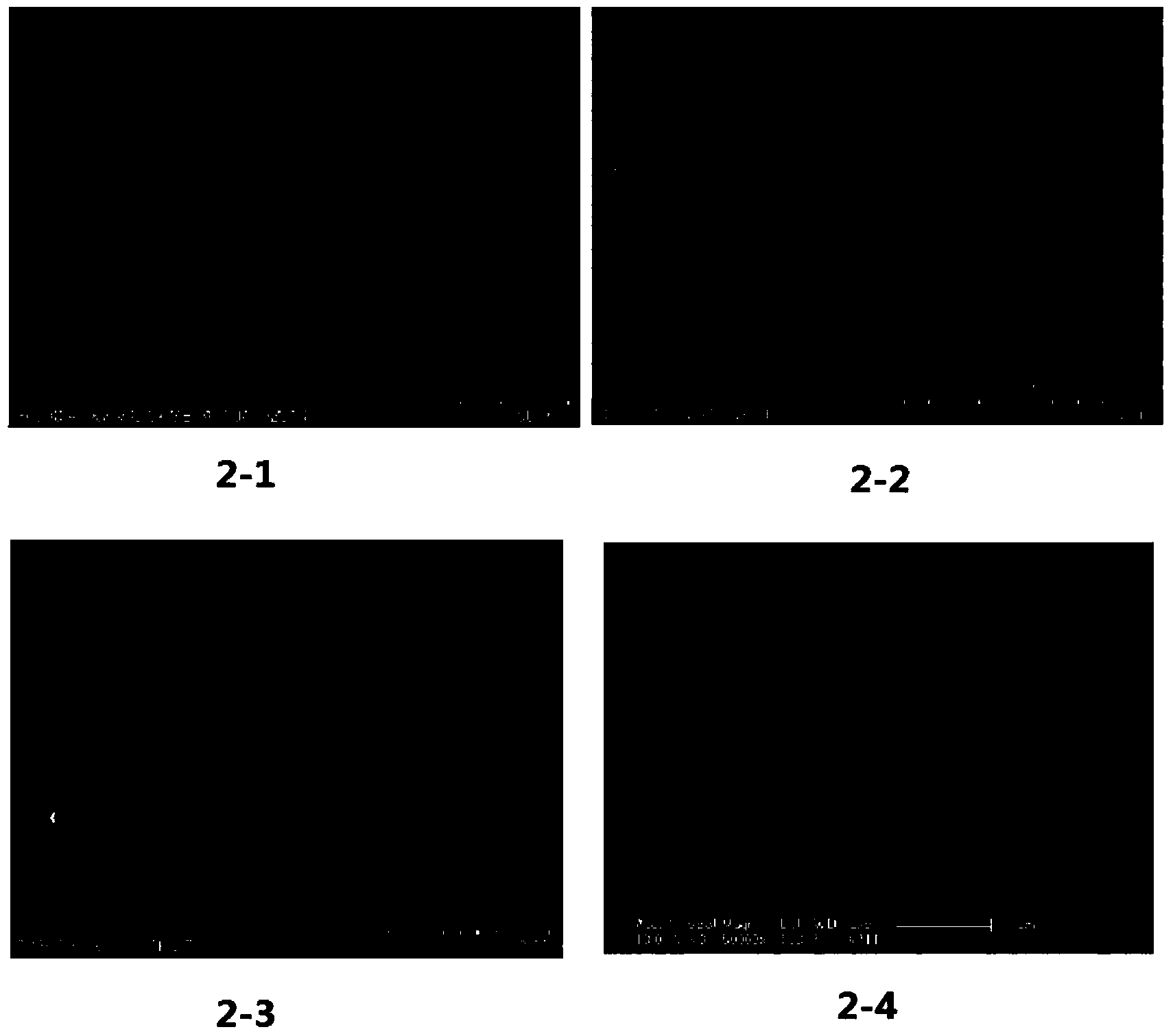
[0128] figure 2 — Figure 4 It is a related diagram of an embodiment of the preparation method of the textured surface of the column array structure and the textured surface of the cone array structure of the present invention. This example uses a self-assembled periodic array of 300 nm diameter polystyrene spheres (PS spheres) to prepare a pillar array structured texture and a cone array structured texture.

[0129] This example uses a c-Si (single crystal silicon) sheet with a thickness of 625 μm (100) crystal plane, the resistivity is 1-10 Ωcm, and the area is 2×2 cm. Using acetone, alcohol, and deionized water, the silicon substrate was cleaned in an ultrasonic cleaning apparatus in sequence, and the time for each cleaning step was 5-10 minutes; the drift method in self-assembly was used to complete the PS ball with a diameter of 300 nm. Self-assembly on the surface of deionized water to form a layer of small spherical film arranged in an orderly period, the film shows ...


PUM

PropertyMeasurementUnit
Diameteraaaaaaaaaa
Vertical heightaaaaaaaaaa
Bottom diameteraaaaaaaaaa

Abstract

The invention provides an array structure fabric surface and a preparing method and application thereof. According to the preparing method for a conical array structure fabric surface, the surface of a semiconductor substrate is paved with a single polymeric microsphere thin film layer, a pillar array structure is etched on the surface of the semiconductor substrate with the polymeric microsphere as a protection layer, a foundation pillar in the semiconductor substrate is oxidized, and an oxidation layer is removed to obtain the fabric surface of a conical array structure. The specific surface area of the fabric surface of the conical array structure manufactured through the method is small, the surface recombination possibility of a photon-generated carrier is low, the preparing technology of the array structure fabric structure is simple, a template is not needed, cost is low, and the defects that in the prior art, large-scale generation cannot be achieved, the preparing steps are complex, and cost is high are overcome.

Description

technical field [0001] The invention relates to the field of micro-nano processing, in particular to an array structure textured surface and its preparation method and application. Background technique [0002] Nanoscience and technology is concerned with the preparation and characterization of physical structures with dimensions in the nanometer range. The resolution limit of ordinary optical lithography is 200nm, so at present, X-ray lithography (X-ray lithography, XRL) technology and electron beam lithography (Electron-Beam Lithography, EBL) are usually used to make nano-sized units, where XRL is Parallel processing mode, the accuracy is generally 20 ~ 50nm; while EBL is serial processing mode, the limit accuracy is 1 ~ 2nm, but the etching speed is only 1cm2 / s, which is not conducive to commercial applications, because the parallel processing of EBL accuracy and XRL Combining capabilities, scanning tunneling microscopy (STM)-based nanolithography has been developed, but...

Claims


Application Information

Patent Timeline
IPC IPC(8): H01L31/028H01L31/18B82Y30/00B82Y40/00B82Y20/00
CPCC30B29/06C30B33/12H01L31/02363Y02E10/547Y02P70/50
Inventor 叶继春李思众高平奇韩灿
Owner NINGBO INST OF MATERIALS TECH & ENG CHINESE ACADEMY OF SCI
Why Eureka
Try Eureka