

Manufacturing method of transparent conducting film and transparent conducting film
A technology of transparent conductive film and manufacturing method, which is applied in the direction of cable/conductor manufacturing, conductive layer on insulating carrier, circuit, etc., and can solve the problem of curling of transparent substrate and decrease of light transmittance of substrate, high cost of transparent conductive film, transparent substrate Large damage and other problems, to achieve the effect of enhanced stability, low production cost, and low overall cost
- Summary
- Abstract
- Description
- Claims
- Application Information
AI Technical Summary
Problems solved by technology
Method used
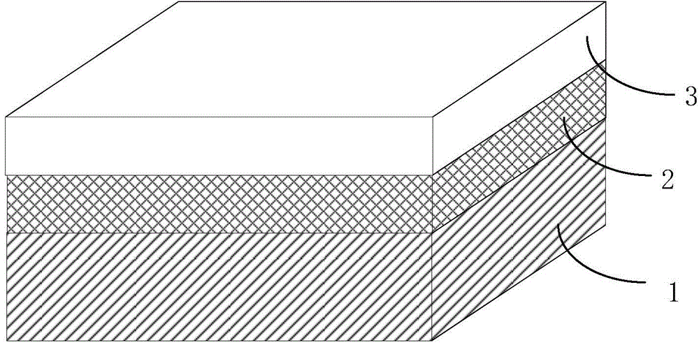
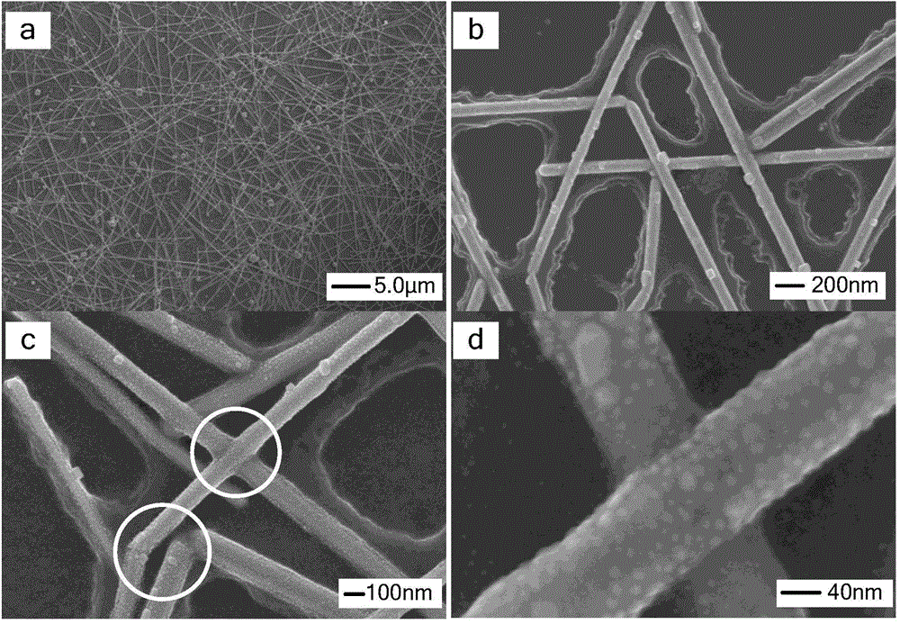
Image

Examples
Embodiment Construction
[0014] The present invention will be described in further detail below in combination with specific embodiments and with reference to the accompanying drawings.
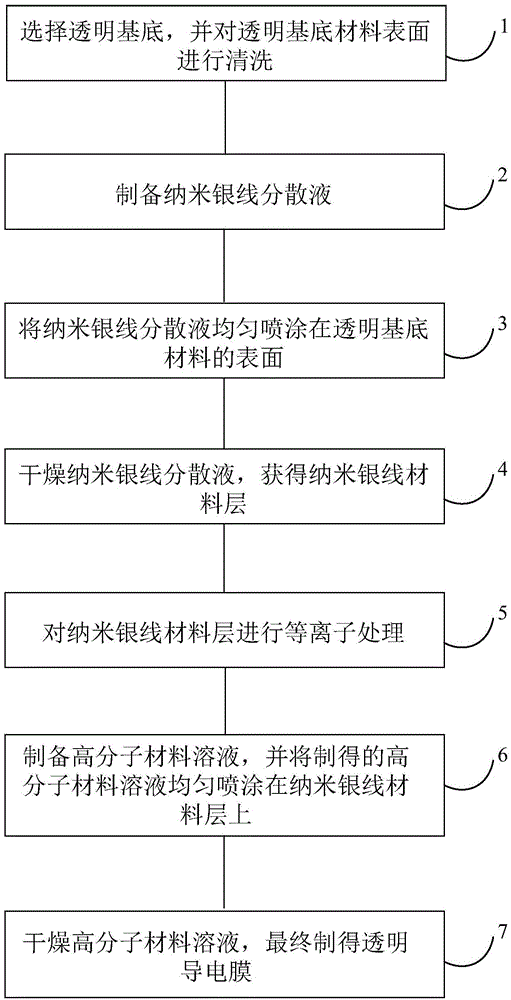
[0015] like figure 1 As shown, it is a flow chart of the manufacturing method of the transparent conductive film in this specific embodiment, including the following steps:
[0016] 1) Select a transparent substrate, and clean the surface of the transparent substrate material. The transparent substrate can be a copolymer of one or more of glass, polycarbonate, polyester, polyacrylate, polyurethane, or a mixture, or a laminate. Preferably, in this step, a plasma cleaning machine can be used to carry out plasma cleaning on the surface of the transparent substrate material, which can improve the surface state of the transparent substrate, thereby improving the spreadability of the spray solution on the surface of the transparent substrate in subsequent steps, thereby facilitating the uniform spraying of the solution o...
PUM
| Property | Measurement | Unit |
|---|---|---|
| thickness | aaaaa | aaaaa |
| diameter | aaaaa | aaaaa |
| thickness | aaaaa | aaaaa |
Abstract
Description
Claims
Application Information