Rectangular patterned Si substrate AlN template for GaN semiconductor material epitaxy and preparation method of rectangular patterned Si substrate AlN template

A semiconductor and patterning technology, applied in semiconductor/solid-state device manufacturing, semiconductor devices, chemical instruments and methods, etc., can solve problems such as cracks in GaN thin films, achieve low cost, high product quality, and improve crystal quality.

Active Publication Date: 2014-09-03
广州市艾佛光通科技有限公司
View PDF8 Cites 14 Cited by
  • Summary
  • Abstract
  • Description
  • Claims
  • Application Information

AI Technical Summary

Problems solved by technology

[0006] In order to solve the crack problem of GaN film caused by the thermal mismatch between GaN and Si substrate in the process of epitaxial GaN-based semiconductor material on the existing Si substrate, and the melting back caused by the alloy eutectic between Ga and Si Etching problem, the present invention provides a low-cost, high-quality, stable epitaxial growth of a rectangular patterned Si substrate AlN template for GaN semiconductor material epitaxy and its preparation method

Method used


Image

  • Rectangular patterned Si substrate AlN template for GaN semiconductor material epitaxy and preparation method of rectangular patterned Si substrate AlN template
  • Rectangular patterned Si substrate AlN template for GaN semiconductor material epitaxy and preparation method of rectangular patterned Si substrate AlN template
  • Rectangular patterned Si substrate AlN template for GaN semiconductor material epitaxy and preparation method of rectangular patterned Si substrate AlN template

Examples


Embodiment 1

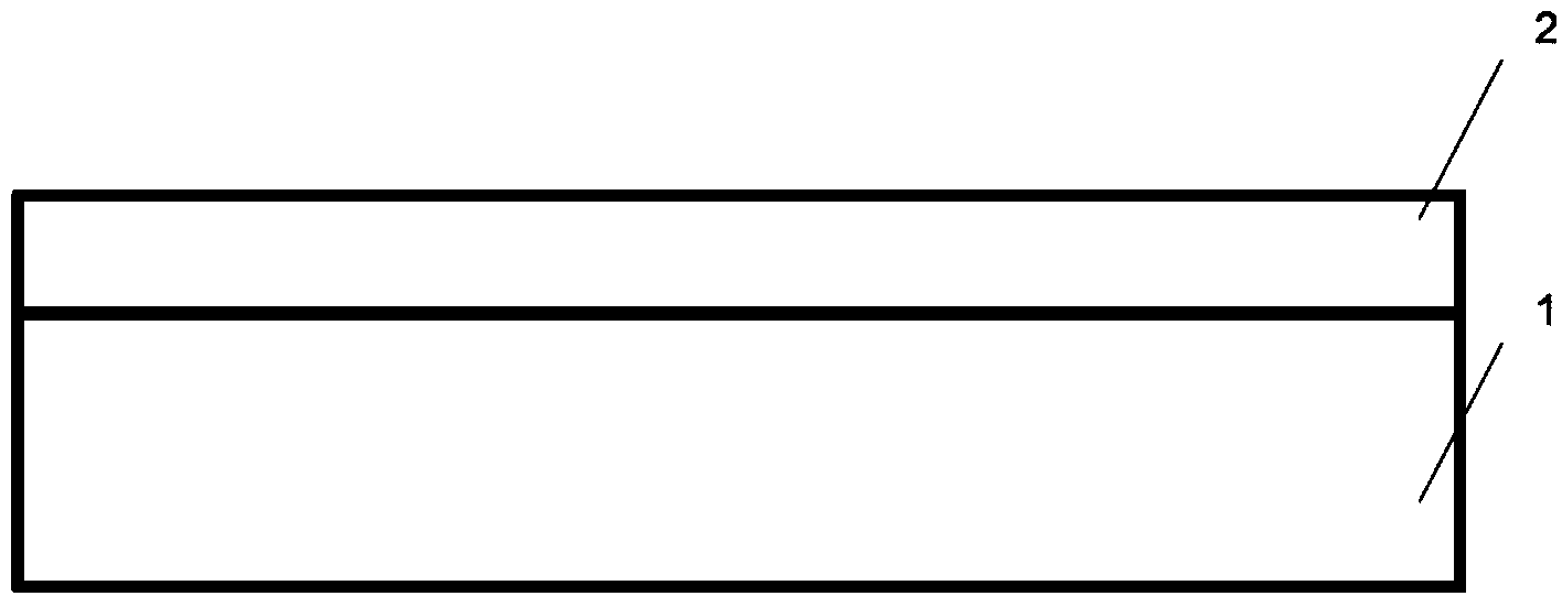
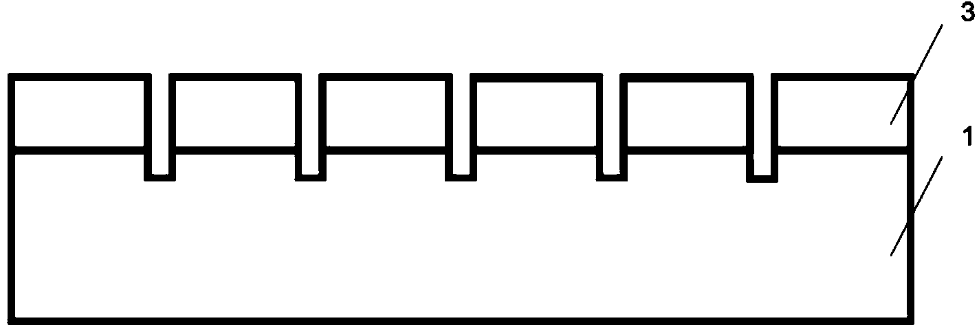
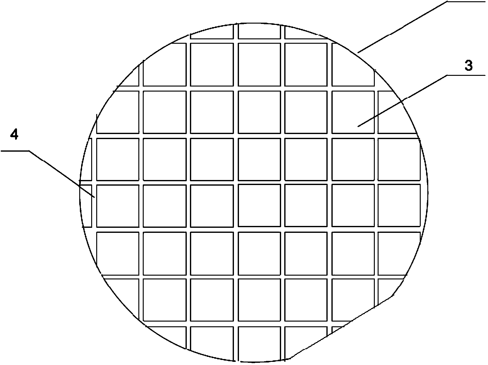
[0030] Attached figure 1 -, 3, a rectangular patterned Si substrate AlN template for epitaxy of GaN semiconductor materials, which includes a Si substrate 1 and a (111) crystal plane on the Si substrate 1 as an AlN template layer for crystal orientation epitaxial growth 2. A plurality of strip-shaped trenches 4 perpendicular to each other are etched on the AlN template layer 1 to form a plurality of mutually independent rectangular platforms 3. The thickness of the AlN template 2 layer is 50nm; the size of the rectangular platform 3 is 1mm×1mm, the width of the strip groove 4 is 10μm and the depth is 8μm

[0031] It is prepared by the following method, including the following steps in sequence:

[0032] a. Clean the Si substrate.

[0033] b. Using the (111) crystal plane of the Si substrate as the crystal orientation, an AlN template layer is grown on the Si substrate by pulsed laser deposition process: the pulsed laser deposition process taste: the substrate temperature is 650℃, an...

Embodiment 2

[0036] This embodiment is modified on the basis of Embodiment 1, and the difference is that the size of the rectangular platform of the rectangular AlN template layer used is 0.5 μm×0.5 μm.

Embodiment 3

[0038] Attached Figure 4-6 Using the rectangular patterned Si substrate AlN template for epitaxy of GaN semiconductor materials of Example 1, a GaN film grown on the Si substrate is prepared, which includes Si substrate 1, AlN template layer 2, and from bottom to top. Intermediate layer 5 and GaN epitaxial layer 6, in which the intermediate layer is Al from bottom to top x Ga 1-x N buffer layer, AlN / GaN insertion layer, SiN x Insertion layer, GaN nucleation layer. Including it is prepared by the following method: the rectangular patterned Si substrate AlN template for epitaxy of GaN semiconductor material prepared in Example 1 is placed in a metal organic chemical vapor deposition reaction chamber, and Al is epitaxially grown in sequence. x Ga 1-x N buffer layer, AlN / GaN insertion layer, SiN x Insertion layer, GaN nucleation layer and GaN epitaxial layer, where Al x Ga 1-x N buffer layer, AlN / GaN insertion layer, SiN x The insertion layer and the GaN nucleation layer constitute ...


PUM

PropertyMeasurementUnit
thicknessaaaaaaaaaa
thicknessaaaaaaaaaa

Abstract

The invention relates to a rectangular patterned Si substrate AlN template for a GaN semiconductor material epitaxy. The rectangular patterned Si substrate AlN template comprises a Si substrate and an AlN template layer epitaxially growing on the Si substrate with a crystal plane (111) as a crystal orientation, a plurality of mutually perpendicular strip-shaped grooves are etched on the AlN template layer to form a plurality of rectangular platforms which are independent with each other. The invention also relates to a method for preparing the patterned Si substrate AlN template. The method comprises the following steps of cleaning the substrate, growing the AlN layer and etching the rectangular platform. According to the rectangular patterned Si substrate AlN template for the GaN semiconductor material epitaxy, the yield is high and the cost is low, the prepared products have good uniformity and high quality.

Description

Technical field [0001] The invention relates to a patterned Si substrate AlN template for epitaxy of GaN semiconductor material and a preparation method thereof, in particular to a rectangular patterned Si substrate AlN template for epitaxy of GaN semiconductor material and a preparation method thereof. Background technique [0002] As one of the representatives of third-generation semiconductor materials, GaN has excellent properties such as direct band gap, wide band gap, high saturation electron drift speed, high breakdown electric field and high thermal conductivity, and has also received extensive attention in microelectronic applications. Since I. Akasaki successfully obtained p-GaN for the first time and achieved a new breakthrough in blue LEDs, GaN-based compound semiconductors have been attracting attention and have been widely used in indoor lighting, commercial lighting, engineering lighting and other fields. [0003] High-quality GaN materials are generally produced by ...

Claims


Application Information

Patent Timeline
Patent Type & Authority Applications(China)
IPC IPC(8): C30B23/04C30B29/40H01L33/02H01L21/02
Inventor 李国强
Owner 广州市艾佛光通科技有限公司
Why Eureka
Try Eureka