Improved radiating GaAs-based terahertz frequency doubling Schottky diode

An improved technology of Schottky diodes, which is applied in the direction of electrical components, circuits, semiconductor devices, etc., can solve the problems of poor heat dissipation and low frequency doubling efficiency of Schottky diodes, etc.

Inactive Publication Date: 2014-09-03
THE 13TH RES INST OF CHINA ELECTRONICS TECH GRP CORP
View PDF4 Cites 12 Cited by
  • Summary
  • Abstract
  • Description
  • Claims
  • Application Information

AI Technical Summary

Problems solved by technology

The existing technology uses silicon dioxide as a passivation layer, and its heat dissipa

Method used


Image

  • Improved radiating GaAs-based terahertz frequency doubling Schottky diode
  • Improved radiating GaAs-based terahertz frequency doubling Schottky diode

Examples


Embodiment Construction

[0013] The present invention will be further described in detail below in conjunction with the accompanying drawings and specific embodiments.

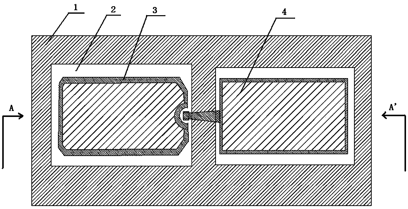
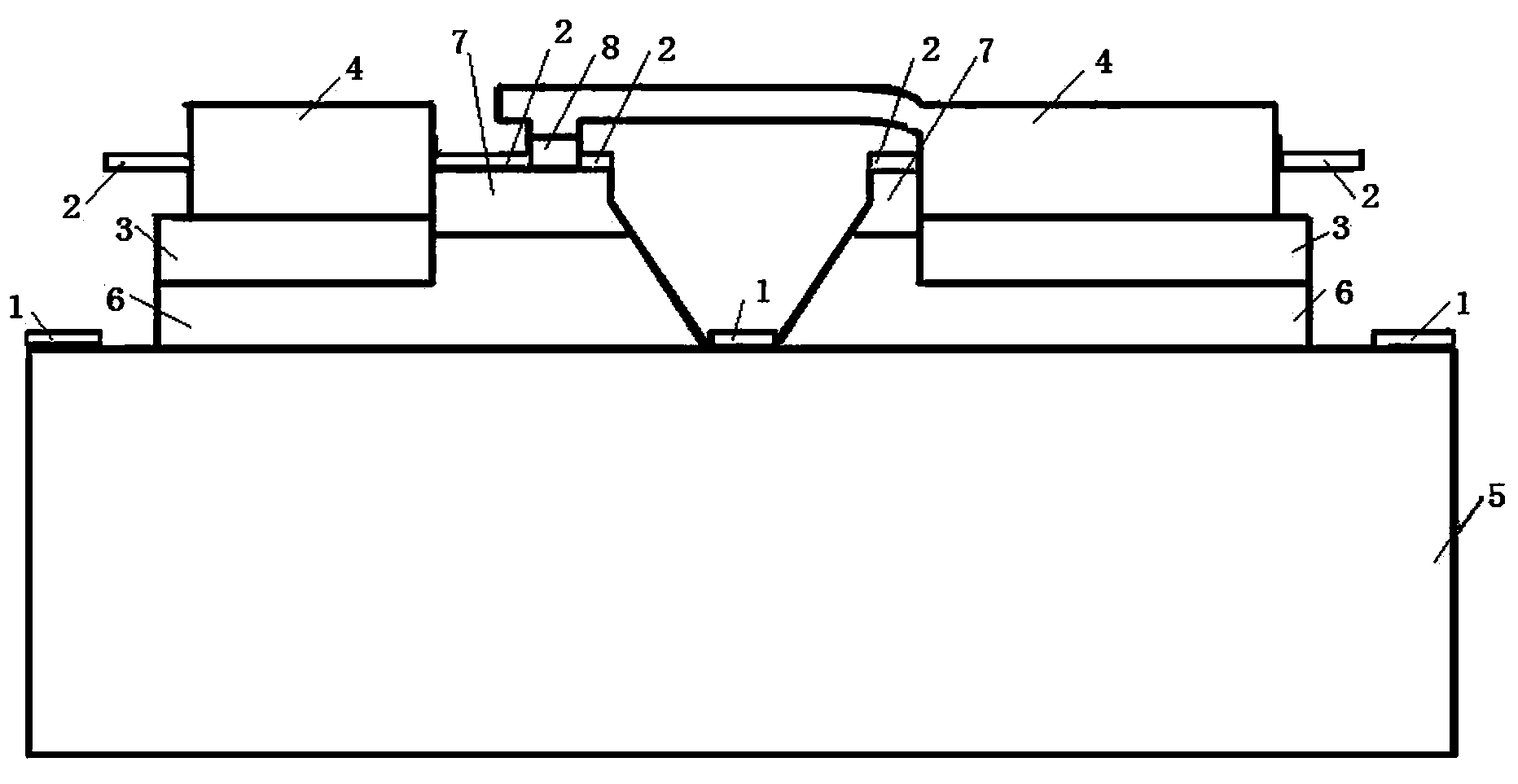
[0014] Such as figure 1 , 2 As shown, a thermally improved GaAs-based terahertz frequency doubling Schottky diode,

[0015] It includes a semi-insulating GaAs substrate 5, a heavily doped GaAs layer 6 on the semi-insulating GaAs substrate 5, a low-doped GaAs layer 7 on the heavily doped GaAs layer 6, a silicon dioxide layer 2, and an ohmic contact metal layer 3 and passivation layer 1. The semi-insulating GaAs substrate 5 is located at the bottom of the terahertz frequency doubling Schottky diode to support the entire terahertz frequency doubling Schottky diode. On the semi-insulating GaAs substrate 5, there is an epitaxially grown heavily doped GaAs layer 6, on the heavily doped GaAs layer 6 there is an epitaxially grown lowly doped GaAs layer 7, and on the lowly doped GaAs layer 7 there is a Schottky contact Metal layer 8, Schot...


PUM

PropertyMeasurementUnit
Thicknessaaaaaaaaaa

Abstract

The invention discloses an improved radiating GaAs-based terahertz frequency doubling Schottky diode, and relates to the technical field of terahertz frequency doubling Schottky diodes. The improved radiating GaAs-based terahertz frequency doubling Schottky diode comprises a semi-insulating GaAs substrate, heavily-doped GaAs layers arranged on the semi-insulating GaAs substrate, lightly-doped GaAs layers arranged on the heavily-doped GaAs layers, silicon dioxide layers, ohmic contact metal layers and passivation layers. The improved radiating GaAs-based terahertz frequency doubling Schottky diode is characterized in that all the passivation layers are made of adamas. According to the improved radiating GaAs-based terahertz frequency doubling Schottky diode, the adamas which is high in heat conductance is used as the passivation layers of the terahertz frequency doubling Schottky diode, so that the radiating performance of the Schottky diode is greatly improved, and the frequency doubling efficiency of the Schottky diode is improved.

Description

technical field [0001] The invention relates to the technical field of Schottky diodes in the terahertz frequency band. Background technique [0002] In the low-end range of terahertz (THz) frequencies, solid-state sources are usually obtained by frequency doubling of semiconductor devices. This method doubles the frequency of the millimeter wave to the THz frequency band through a nonlinear semiconductor device, and has the advantages of compact structure, easy adjustment, long life, controllable waveform, and normal temperature operation. At present, short-wavelength submillimeter wave and THz solid-state sources are mainly obtained by frequency doubling. The use of Schottky diode devices to achieve high-efficiency frequency multiplication not only has a simple circuit structure and high frequency multiplication efficiency, but also has the advantages of high output power of the oscillation source, high frequency stability of the frequency multiplication amplifier chain, ...

Claims


Application Information

Patent Timeline
IPC IPC(8): H01L29/872H01L29/16
CPCH01L29/872H01L23/298H01L23/3738
Inventor 王俊龙王晶晶邢东梁士雄张立森杨大宝赵向阳冯志红
Owner THE 13TH RES INST OF CHINA ELECTRONICS TECH GRP CORP
Why Eureka
Try Eureka