Storage controller

A storage controller and memory technology, used in instruments, electrical digital data processing, energy-saving computing, etc., can solve the problems of reduced reading speed and high power consumption, and achieve the effects of small unit size, low power consumption, and low cost

Active Publication Date: 2014-09-10
SHANGHAI XINCHU INTEGRATED CIRCUIT
View PDF9 Cites 6 Cited by
  • Summary
  • Abstract
  • Description
  • Claims
  • Application Information

AI Technical Summary

Problems solved by technology

The external data buffer is generally SRAM structure or DRAM chip. Although the capacity is increased, the power consumption is still very large, especially for DRAM, which needs to be refreshed regularly to keep the data intact. will be reduced

Method used


Image

  • Storage controller
  • Storage controller
  • Storage controller

Examples


Embodiment 1

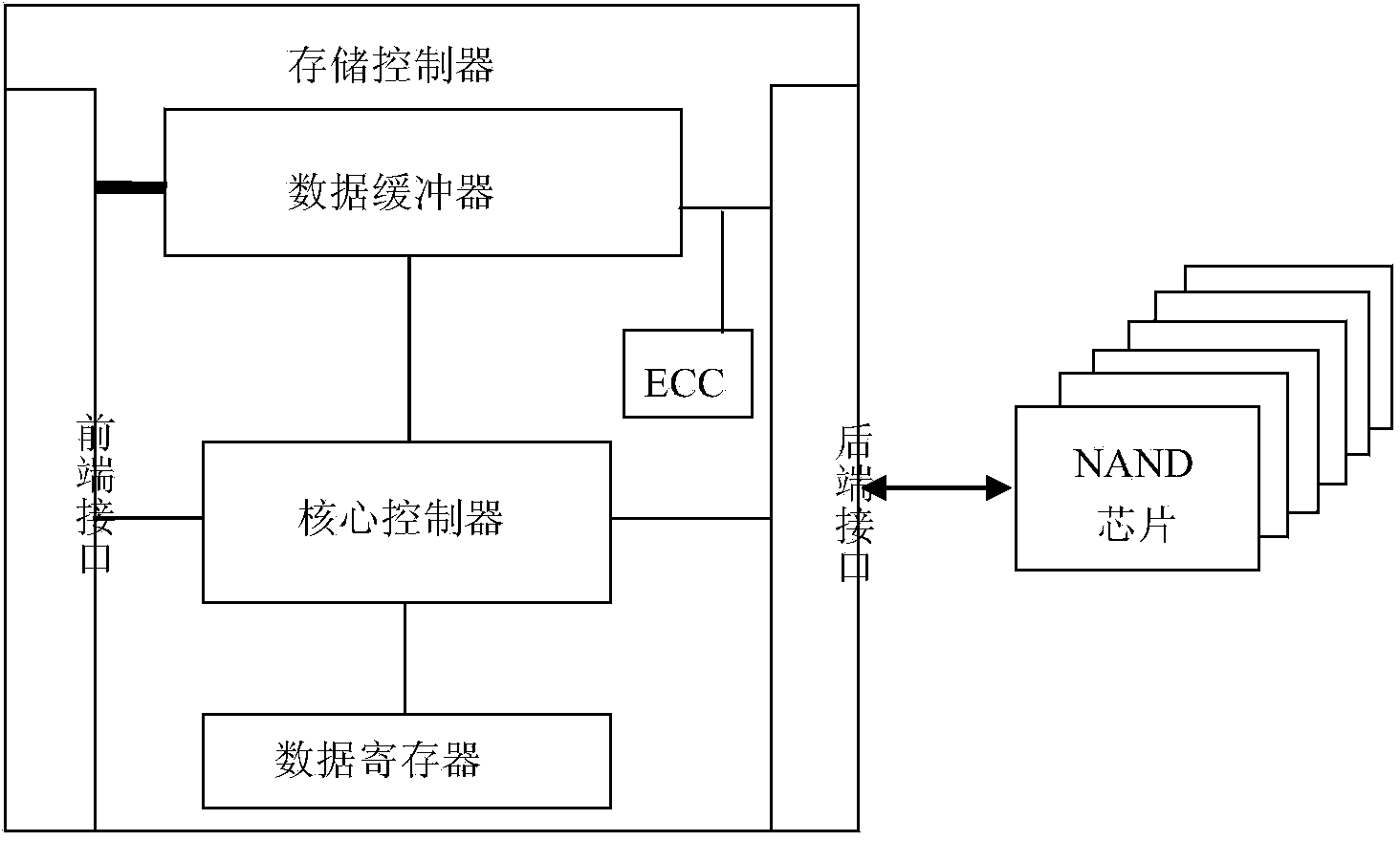
[0026] The invention discloses a storage controller, which is suitable for an operating system to process data on an external storage device. refer to image 3 As shown, it includes a data buffer module (buffer), a data register module (register) and a core controller module (MCU). Both the data buffer module and the data register module are connected to the core controller module. The operating system sends operating instructions to the controller core module, and the core controller module performs data reading, writing, erasing and / or address mapping on the NAND chipset according to the instructions it receives, and performs data processing on the external storage device. Balanced loss control and DMA control operations, further, the controller core module optimizes the data interaction between the operating system and the external memory through the data buffer module according to the received operation instructions.

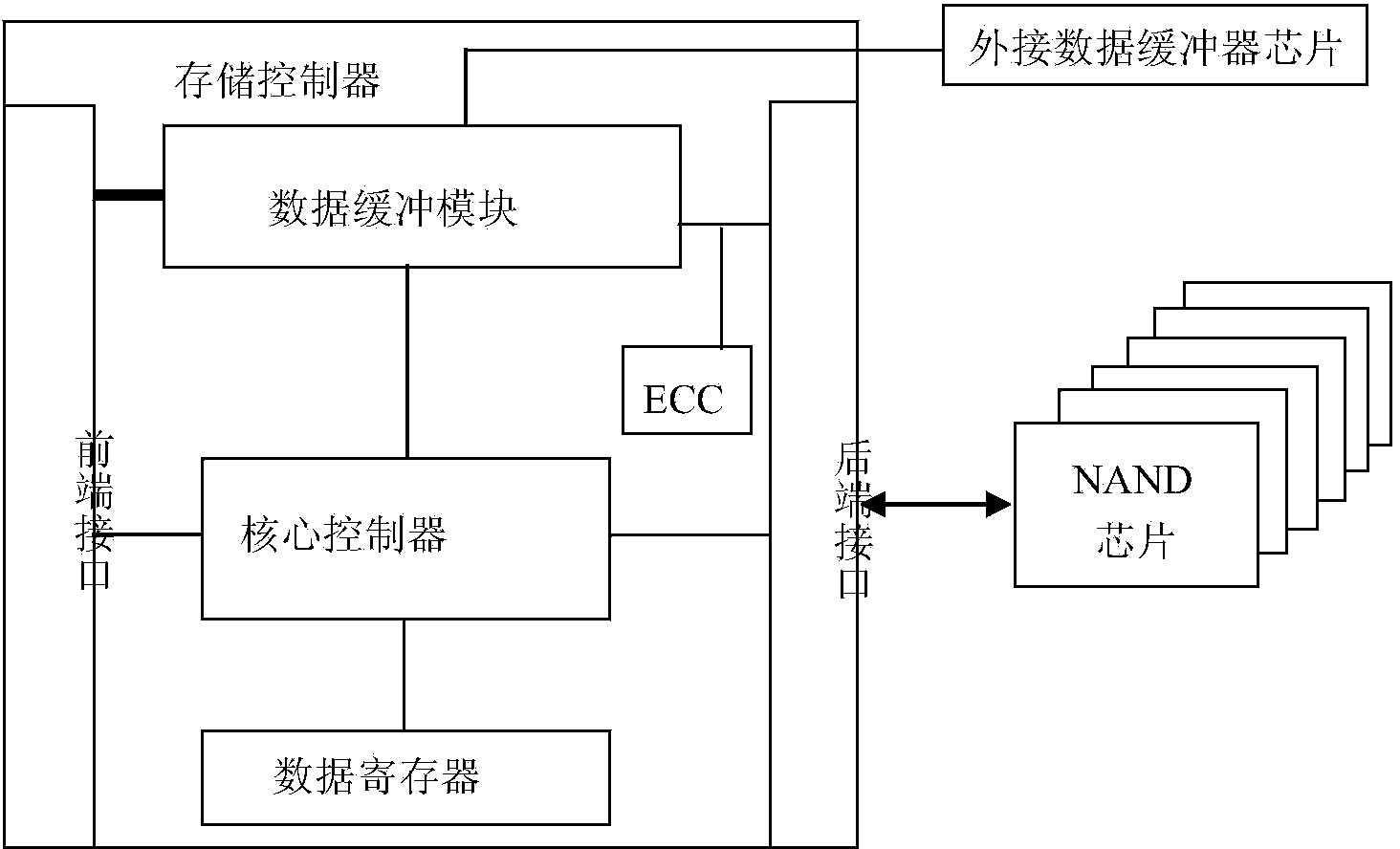
[0027] The storage controller is also provided with a...

Embodiment 2

[0039] A specific embodiment is given below for further elaboration.

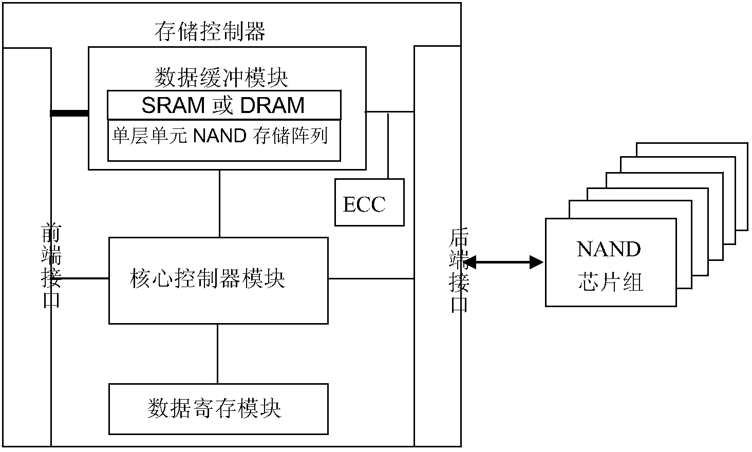
[0040] Assuming that for a 2bit multi-level cell NAND solid state drive per unit, the internal storage controller chip can integrate a single-level cell NAND storage array to replace all traditional data buffers. The structure of the entire solid state drive is as follows: Figure 4 shown. When the system reads data from the SSD, the sequence is: (1) the storage controller accepts the command and reads the page data from the 2bit multi-layer unit NAND chip per unit through the back-end bus; (2) saves the page data to the single (3) The system reads I / O data from the NAND data buffer of the single-layer unit through the front-side bus. When the system writes data to the SSD, the sequence is: (1) the system transmits the data to be written through the front-side bus; (2) saves the I / O data to be written into the single-layer unit NAND data buffer; (3) The storage controller accepts the command and writes th...


PUM


Abstract

The invention provides a storage controller. A single-layer cell storage array is integrated into the storage controller and replaces part or all of data buffers, so that the integrated single-layer cell NAND storage array has the advantages of being small in storage unit size, low in cost, low in power consumption, nonvolatile and the like, and the novel NAND storage controller of the structure is suitable for the application field with high requirements on power consumption, cost or capacity. In addition, if a certain application environment has quite high requirements on speed, the single-layer cell NAND array can be taken as a second-stage data buffer to be together with a first-stage SRAM or DRAM buffer to form a mixed data buffer, so that the objective of high-speed reading and writing is achieved, and the advantages of small cell size, low cost, low power consumption, nonvolatility and the like are realized.

Description

technical field [0001] The invention relates to the field of semiconductors, in particular to a storage controller, which can realize high-speed data cache. Background technique [0002] NAND solid-state drives have become the mainstream non-volatile storage technology and are widely used in various fields such as data centers, personal computers, mobile phones, smart terminals, and consumer electronics, and the demand is still growing. The manufacturing process of NAND solid-state drives has also been developed to 16nm, transforming from a two-dimensional manufacturing process to a three-dimensional manufacturing process. Samsung has announced the commercial production of 128Gb24 unit (bit) stacked three-dimensional NAND chips. Micron announced a new 16nm128Gb two-dimensional NAND chip, using a new two-dimensional cell structure to break through the size reduction limit of the traditional two-dimensional structure. [0003] Traditional NAND SSD storage chips and memory co...

Claims


Application Information

Patent Timeline
Patent Type & Authority Applications(China)
IPC IPC(8): G06F13/16G06F3/06
CPCY02D10/00
Inventor 景蔚亮陈邦明
Owner SHANGHAI XINCHU INTEGRATED CIRCUIT
Why Eureka
Try Eureka