Self-aligned metal oxide thin film transistor device and manufacturing method

A technology of oxide film and manufacturing method, applied in semiconductor/solid-state device manufacturing, transistors, electric solid-state devices, etc., can solve problems such as complex processes that are prone to parasitic capacitance, so as to reduce parasitic capacitance, achieve minimization, and reduce manufacturing effect of difficulty

Active Publication Date: 2017-04-19
SHENZHEN ROYOLE TECH CO LTD
View PDF6 Cites 0 Cited by
  • Summary
  • Abstract
  • Description
  • Claims
  • Application Information

AI Technical Summary

Problems solved by technology

[0007] The purpose of the present invention is to provide a method for manufacturing a self-aligned metal oxide thin film transistor device, which aims to solve the problem that the traditional method is prone to produce parasitic capacitance and the process is complex

Method used


Image

  • Self-aligned metal oxide thin film transistor device and manufacturing method
  • Self-aligned metal oxide thin film transistor device and manufacturing method
  • Self-aligned metal oxide thin film transistor device and manufacturing method

Examples


Embodiment 2

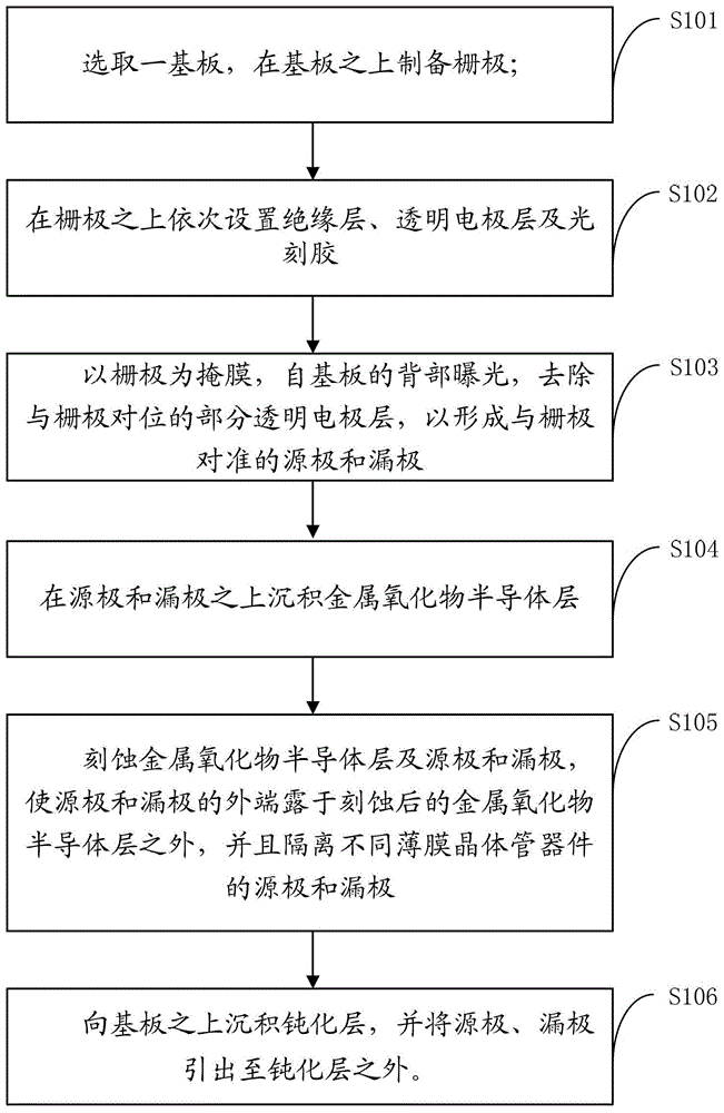
[0075] Figure 5 It shows the flow chart of the method for manufacturing the self-aligned metal oxide thin film transistor pixel circuit provided by the second embodiment of the present invention, Figure 6-1~6-10 A schematic structural diagram corresponding to the manufacturing method is shown, and for convenience of description, only parts related to this embodiment are shown.

[0076] Such as Figure 5 , the method includes the following steps:

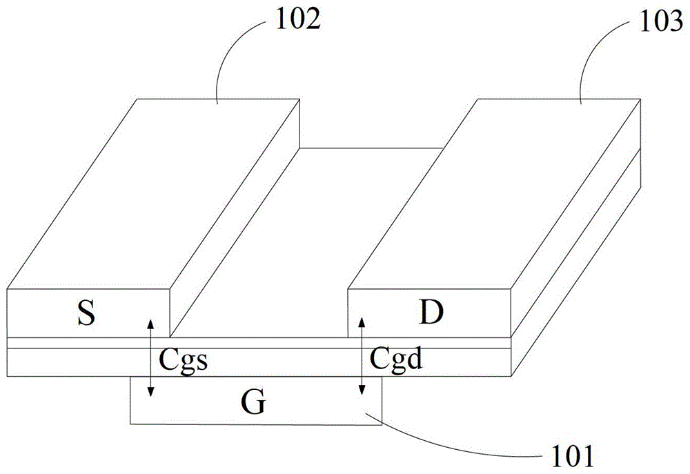
[0077] In step S201, a substrate 21 is selected, and a gate 221, a gate lead 222 and a storage capacitor electrode 223 are prepared on the substrate 21; Figure 6-1 .

[0078] In this step, the substrate 21 is made of a transparent material. "Transparent" in this embodiment refers to a material that is transparent to the light wave used in the photolithography process, and then the first photolithography mask is used to make the gate 221, the gate Lead wire 222 and storage capacitor electrode 223 . Optionally, a buffer layer m...


PUM


Abstract

Provided is a method for producing a self-aligned metal oxide thin-film transistor (TFT) component, which comprises: selecting a substrate (11), and preparing a gate electrode (12) on the substrate (11); arranging an insulation layer (13), a transparent electrode layer (14) and photoresist (15) in sequence on the gate electrode (12); using the gate electrode (12) as a mask, and exposing from a back of the substrate (11) to form source and drain electrodes (141, 142) that are aligned with the gate electrode (12); depositing a metal oxide semiconductor layer (17) on the transparent electrode layer (14); etching the semiconductor layer (17) and the source and drain electrodes (141, 142) to make outer ends of the source and drain electrodes (141, 142) come out of the metal oxide semiconductor layer; depositing a passivation layer (18), and leading out the source and drain electrodes (141, 142). The component uses a transparent conductor as an electrode layer, uses a bottom gate as a mask to perform back exposure, and etches the source and drain electrodes, which implements self-alignment between the source and drain electrodes and the gate electrode, effectively reduces parasitic capacitance, and improves component performance. The component is in a bottom gate and bottom contact structure. No etching blocking layer needs to be fabricated, simplifying a process, reducing usage of photolithographic masks, improving efficiency, and improving electrical characteristics of the component.

Description

technical field [0001] The invention belongs to the technical field of electronic devices, in particular to a self-aligned metal oxide thin film transistor device and a manufacturing method thereof. Background technique [0002] Metal oxide thin film transistor (TFT) is a basic circuit component device that can be widely used in various electronic systems, and it has many advantages, such as high electron mobility, low temperature manufacturing process, high stability, high transparency, etc. . Such as figure 1 As shown, in the traditional TFT manufacturing process, the alignment of the gate (Gate) 101, the source (Source) 102, and the drain (Drain) 103 of the TFT device is done manually or mechanically by using two different mask plates. achieved by optical alignment. Due to the limitation of the accuracy of the alignment equipment and other factors, this method will cause a certain overlap between the source 102, the drain 103 and the gate 101, resulting in a large gate...

Claims


Application Information

Patent Timeline
Patent Type & Authority Patents(China)
IPC IPC(8): H01L21/00H01L27/088
CPCH01L29/7869H01L27/1225H01L29/66969
Inventor 魏鹏余晓军刘自鸿
Owner SHENZHEN ROYOLE TECH CO LTD
Why Eureka
Try Eureka