A projected capacitive screen without bridging and its manufacturing method
A manufacturing method and technology of capacitive screen, applied in the field of capacitive screen, can solve the problems of poor shadow elimination effect, difficult to control yield, difficult to control yield, etc., so as to ensure optical transmittance, improve yield, and save bridging process Effect
- Summary
- Abstract
- Description
- Claims
- Application Information
AI Technical Summary
Problems solved by technology
Method used
Image
Examples
Embodiment 1
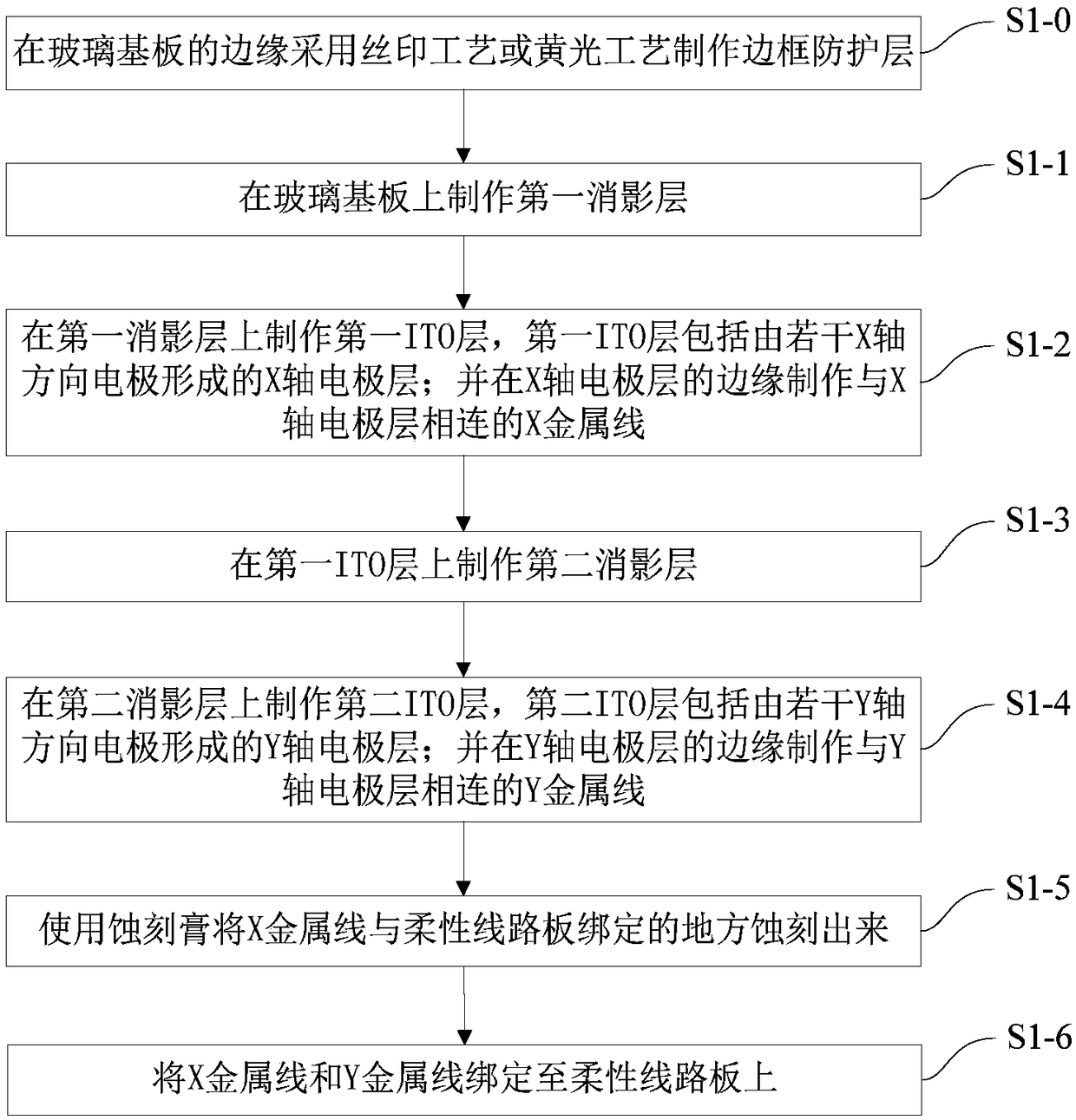
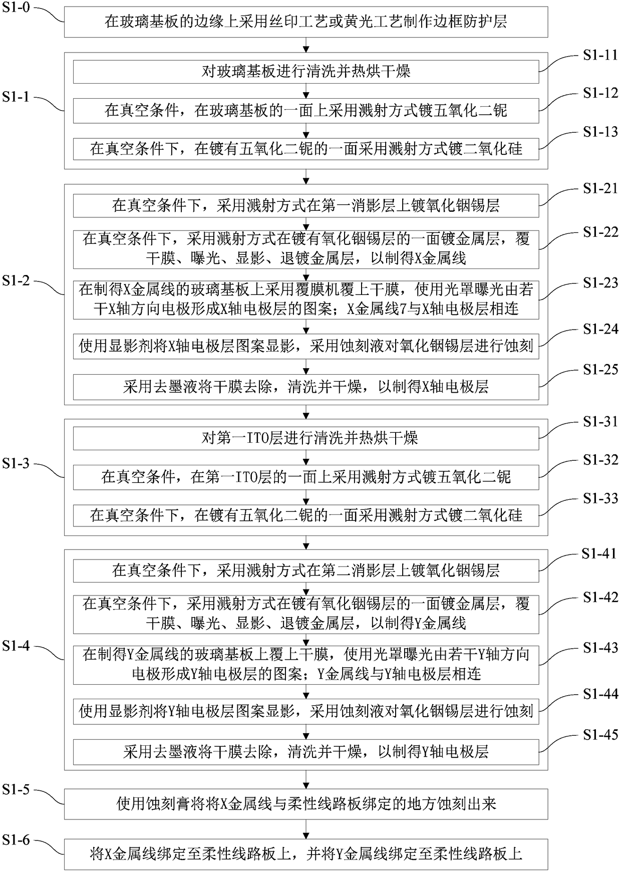
[0081] like figure 2 , image 3 As shown, this embodiment provides a method for manufacturing a projected capacitive screen without bridging, including the following steps:
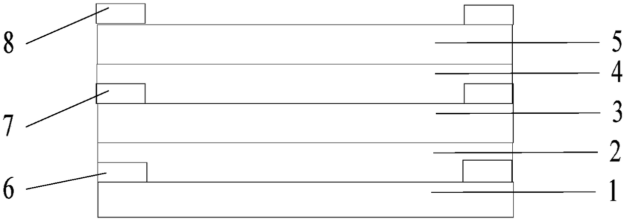
[0082] S1-0: Fabricate the frame protection layer 6 on the edge of the glass substrate 1 by using a silk screen process or a yellow light process. Specifically, the thickness of the frame protection layer 6 is less than 7um, the thinner the better.
[0083] Specifically, the specific steps of making the frame protective layer 6 by using silk screen printing technology: making a base plate on the glass substrate 1, drying board, developing, drying, revision, printing, drying, and finished product; wherein the drying board includes screen selection, frame selection, stretching Netting, drying, coating or attaching photosensitive adhesive, drying and other steps.
[0084] The specific steps for making the frame protective layer 6 using the yellow light process: pre-PR cleaning (that is, the process of re...
Embodiment 2
[0116] like Figure 4 , Figure 5 As shown, this embodiment provides a method for manufacturing a projected capacitive screen without bridging, including the following steps:
[0117] S2-0: Fabricate the frame protective layer 6 on the edge of the glass substrate 1 by using a silk screen process or a yellow light process. Specifically, its specific steps are consistent with step S1-0 in Embodiment 1. Understandably, the thickness of the frame protection layer 6 is less than 7um, the thinner the better.
[0118] S2-1: Fabricate the first image erasing layer 2 on the glass substrate 1 .
[0119] Specifically, step S2-1 includes:
[0120] S2-11: cleaning and drying the glass substrate 1 by heat.
[0121] S2-12: Under vacuum conditions, one side of the glass substrate 1 is sputtered with niobium pentoxide or silicon oxynitride.
[0122] S2-13: Under vacuum conditions, sputtering is used to plate silicon dioxide on the side coated with niobium pentoxide or silicon oxynitride,...
PUM
 Abstract
Description
Claims
Application Information


