Composite anode and manufacturing method thereof, and organic electroluminescent device and manufacturing method thereof
A composite anode, conductive metal technology, applied in the manufacturing of organic semiconductor devices, electric solid state devices, semiconductor/solid state devices, etc., can solve the problems of total reflection loss, refractive index difference, low light output performance, etc., to improve the hole injection ability , the effect of improving conductivity
- Summary
- Abstract
- Description
- Claims
- Application Information
AI Technical Summary
Problems solved by technology
Method used
Image
Examples
Embodiment 1
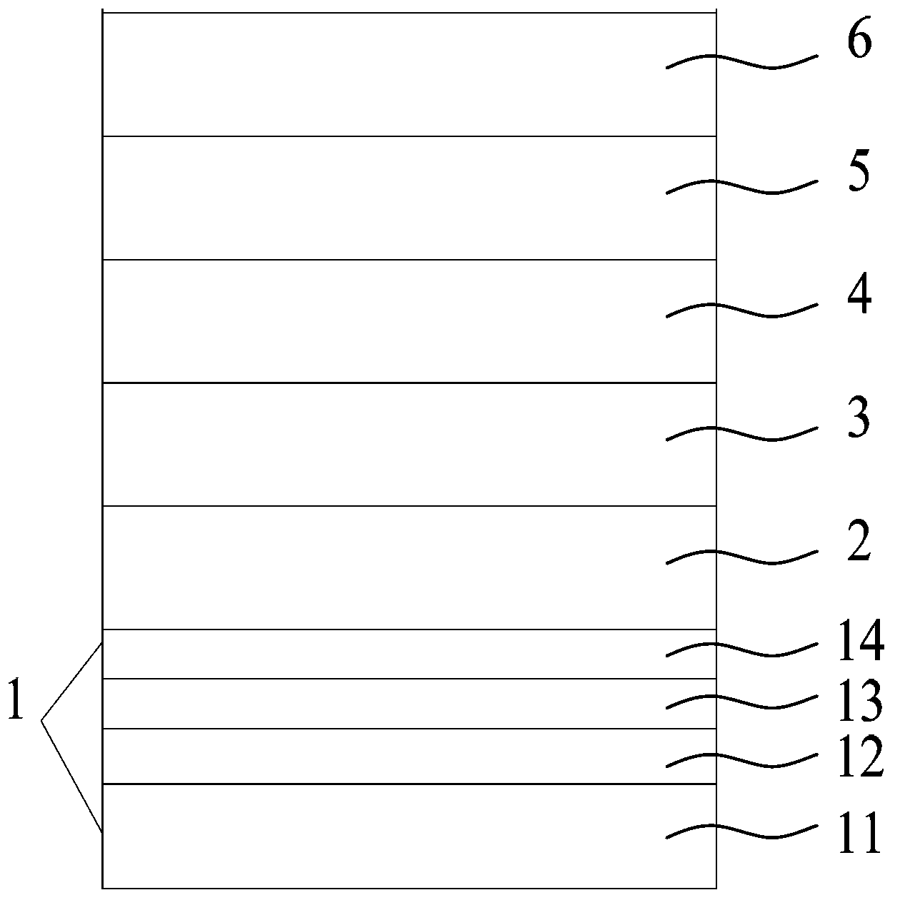
[0057] A method for preparing a composite anode, comprising the following steps:
[0058] (1) First, the glass substrate is subjected to photolithography treatment, and then cut into 2×2cm 2 Then use detergent, deionized water, acetone, ethanol, and isopropanol to sonicate for 15 minutes each to remove organic pollutants on the glass surface, clean and air dry;
[0059] (2) First, the doped metal oxide layer is prepared on the light-emitting surface of the glass substrate by vacuum evaporation, and the material of the doped metal oxide layer is MoO 3 and MgO in a mass ratio of 1:0.2 (expressed as MoO 3 :MgO), the thickness of the doped metal oxide layer is 10nm, and the evaporation pressure is 2×10 -4 Pa, the evaporation rate is 1nm / s; then the conductive metal single substance layer is prepared by evaporation on the doped metal oxide layer, the material of the conductive metal single substance layer is Ag, the thickness is 5nm, and the evaporation pressure is 2×10 -4 Pa, t...
Embodiment 2
[0061] A method for preparing a composite anode, comprising the following steps:
[0062] (1) First, the glass substrate is subjected to photolithography treatment, and then cut into 2×2cm 2 Then use detergent, deionized water, acetone, ethanol, and isopropanol to sonicate for 15 minutes each to remove organic pollutants on the glass surface, clean and air dry;
[0063] (2) First, a doped metal oxide layer was prepared on the light-emitting surface of the glass substrate by vacuum evaporation, and the material of the doped metal oxide layer was WO 3 and MgO according to the mass ratio of 1:0.1 (expressed as WO 3 :MgO), the thickness of the doped metal oxide layer is 20nm, and the evaporation pressure is 3×10 -3 Pa, the evaporation rate is 6nm / s; then, the conductive metal single substance layer is prepared by evaporation on the doped metal oxide layer, the material of the conductive metal single substance layer is Al, the thickness is 20nm, and the evaporation pressure is 3×...
Embodiment 3
[0065] A method for preparing a composite anode, comprising the following steps:
[0066] (1) First, the glass substrate is subjected to photolithography treatment, and then cut into 2×2cm 2 Then use detergent, deionized water, acetone, ethanol, and isopropanol to sonicate for 15 minutes each to remove organic pollutants on the glass surface, clean and air dry;
[0067] (2) Firstly, a doped metal oxide layer is prepared on the light-emitting surface of the glass substrate by vacuum evaporation, and the material of the doped metal oxide layer is V 2 o 5 The mixed material formed with MgO according to the mass ratio of 1:0.3 (expressed as V 2 o 5 :MgO), the thickness of the doped metal oxide layer is 2nm, and the evaporation pressure is 1×10 -3 Pa, the evaporation rate is 10nm / s; then the conductive metal single substance layer is prepared by evaporation on the doped metal oxide layer, the material of the conductive metal single substance layer is Pt, the thickness is 2nm, a...
PUM
| Property | Measurement | Unit |
|---|---|---|
| thickness | aaaaa | aaaaa |
| thickness | aaaaa | aaaaa |
| luminance | aaaaa | aaaaa |
Abstract
Description
Claims
Application Information
 - R&D
- Intellectual Property
- Life Sciences
- Materials
- Tech Scout
- Unparalleled Data Quality
- Higher Quality Content
- 60% Fewer Hallucinations
Browse by: Latest US Patents, China's latest patents, Technical Efficacy Thesaurus, Application Domain, Technology Topic, Popular Technical Reports.
© 2025 PatSnap. All rights reserved.Legal|Privacy policy|Modern Slavery Act Transparency Statement|Sitemap|About US| Contact US: help@patsnap.com


