Method for calculating influence of panel machining errors to electrical property based on partitioning mode
A technology for panel processing and electrical performance, which is applied in computing, electrical digital data processing, special data processing applications, etc.
- Summary
- Abstract
- Description
- Claims
- Application Information
AI Technical Summary
Problems solved by technology
Method used
Image
Examples
Embodiment Construction
[0059] The present invention will be described in further detail below with reference to the accompanying drawings.
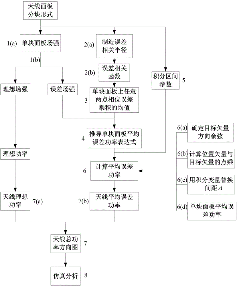
[0060] refer to figure 1 , the concrete steps of the present invention are as follows:
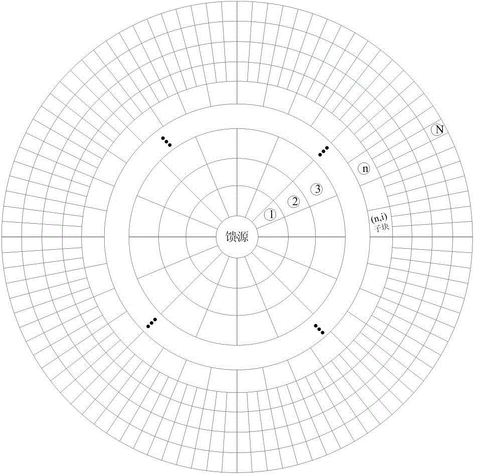
[0061] Step 1, express the far field of a single panel as the sum of the ideal field and the error field; (1a) refer to figure 2 , the reflective surface spliced by panels is divided into N rings, and the nth ring (n=1,2,…,N) can be divided into K n block. There will be manufacturing errors on the surface of each panel. For the (n,i)th panel, assuming that the phase error caused by a random error at a certain point on the surface is δ(ρ), its far-field pattern can be expressed as
[0062] E n , i = ∫ ∫ ( n , i ) ...
PUM
 Abstract
Description
Claims
Application Information


