Etching composition for copper-based metal layer and method of preparing metal line
A technology of composition and metal layer, applied in the field of etchant composition, can solve problems such as electrical short circuit wiring, copper metal layer etching, failure, etc., and achieve the effects of preventing electrical short circuit, preventing residue, and improving the cone angle profile
- Summary
- Abstract
- Description
- Claims
- Application Information
AI Technical Summary
Problems solved by technology
Method used
Image
Examples
Embodiment
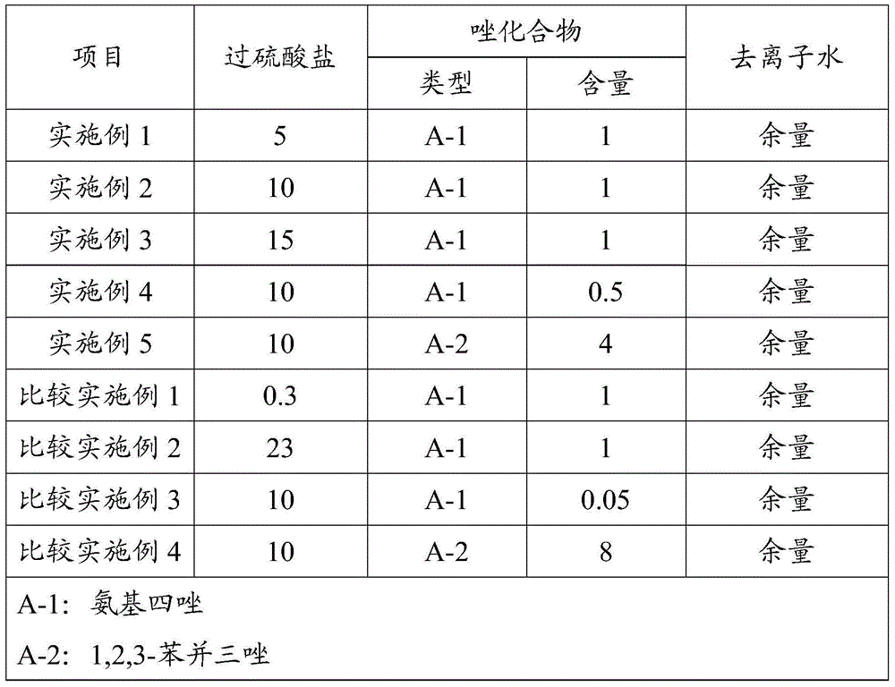
[0124] 1-1. Example 1 to Example 5 and Comparative Example 1 to Comparative Example 4
[0125] According to the components listed in Table 1 below, etchant compositions were prepared in Examples 1 to 5 and Comparative Examples 1 to 4 (unit: weight percent relative to the total weight percent 100%).
[0126] [Table 1]
[0127]
experiment Embodiment 2
[0129] After depositing a metal oxide material (ITO) on a glass substrate (100mm x 100mm) and depositing a copper layer on top of the above layer, a photoresist with a desired pattern is formed on the substrate by photolithography. Then, an etching process was performed on the copper-based metal layer using each of the compositions prepared in Example 1 to Example 5 and Comparative Example 1 to Comparative Example 4, respectively.
[0130] An apparatus in injection etching mode (model name: ETCHER (TFT), SEMES Corporation) was used, and the etchant composition was kept at a temperature of about 30° C. during etching. However, the temperature may be appropriately changed according to other process conditions and other factors, if desired. Etching is typically performed for about 100 seconds, which time may vary depending on the etching temperature. The profile of the copper-based metal layer etched during the etching process was examined using a cross-sectional SEM (scanning e...
experiment Embodiment 3
[0174] After depositing a metal oxide material (ITO) on a glass substrate (100mm x 100mm) and depositing a copper layer on top of the above layer, a photoresist with a desired pattern is formed on the substrate by photolithography. Then, an etching process was performed on the copper-based metal layer using each of the compositions prepared in Example 12 to Example 17 and Comparative Example 11 to Comparative Example 16, respectively.
[0175] A device in injection etching mode (model name: ETCHER (TFT), SEMES Corporation) was used, and the etchant composition was kept at a temperature of about 30 °C during etching. However, the temperature may be appropriately changed according to other process conditions and other factors, if desired. Etching is typically performed for about 100 seconds, which time may vary depending on the etching temperature. The profile of the copper-based metal layer etched during the etching process was examined using a cross-sectional SEM (manufacture...
PUM
| Property | Measurement | Unit |
|---|---|---|
| electrical resistivity | aaaaa | aaaaa |
Abstract
Description
Claims
Application Information


