Array substrate manufacturing method, array substrate and display device

An array substrate and manufacturing method technology, applied in the display field, can solve the problems of low process yield, long manufacturing process time, and high cost, and achieve the effects of reducing process complexity, reducing the number of patterning processes, and reducing process costs

Inactive Publication Date: 2014-10-01
BOE TECH GRP CO LTD
View PDF4 Cites 11 Cited by
  • Summary
  • Abstract
  • Description
  • Claims
  • Application Information

AI Technical Summary

Problems solved by technology

[0013] In view of this, the present invention provides a method for manufacturing an array substrate, an array substrate and a display device, so as to solve the defects of long manufacturing process time, low process yield and high cost of the existing low-temperature polysilicon array substrate.

Method used


Image

  • Array substrate manufacturing method, array substrate and display device
  • Array substrate manufacturing method, array substrate and display device
  • Array substrate manufacturing method, array substrate and display device

Examples


Embodiment Construction

[0066] In order to make the technical problems, technical solutions and advantages to be solved by the present invention clearer, the following will describe in detail with reference to the drawings and specific embodiments.

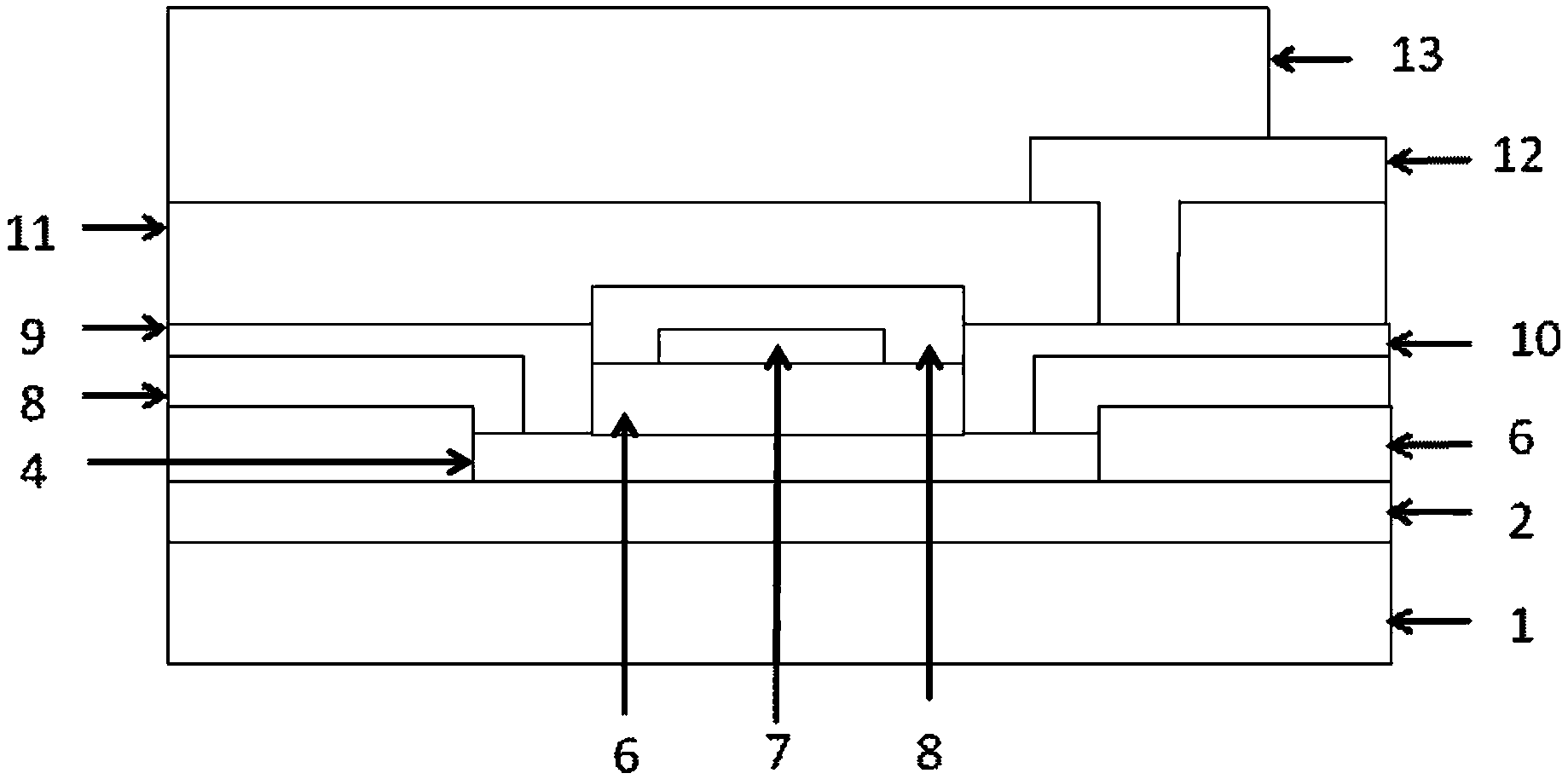
[0067] In order to solve the problems of long manufacturing process time, low process yield and high cost of the existing low-temperature polysilicon array substrate, please refer to image 3 , an embodiment of the present invention provides a method for manufacturing an array substrate, comprising the following steps:

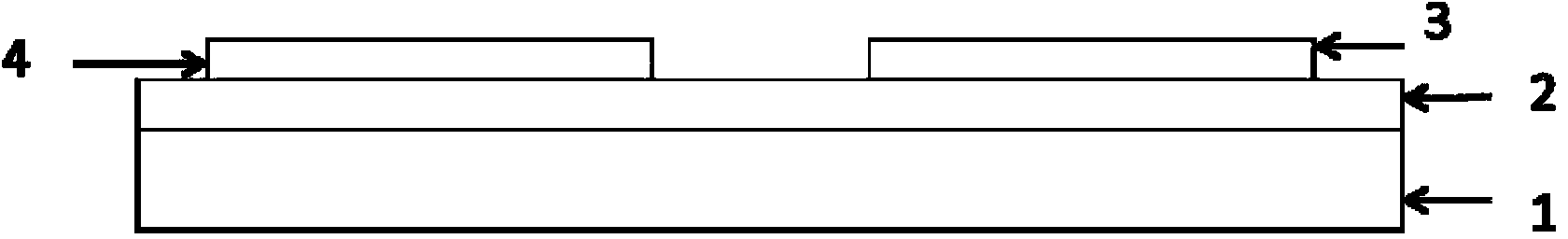
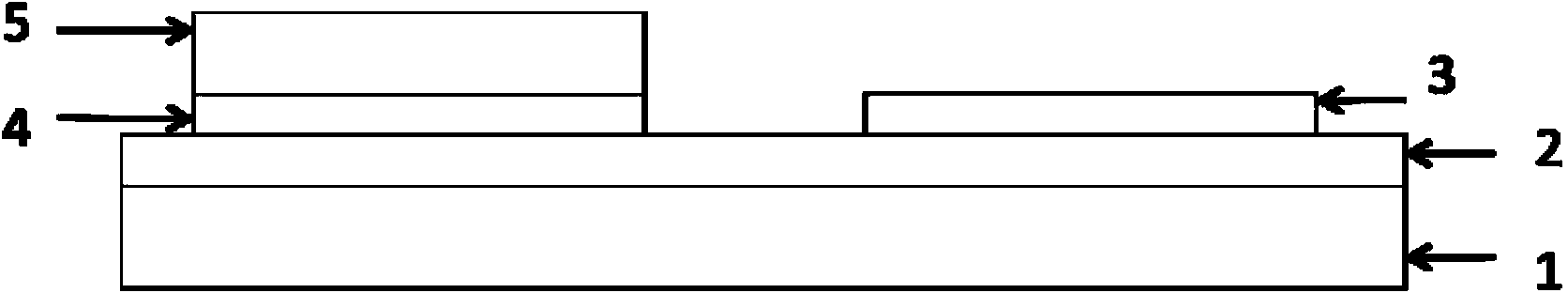
[0068] Step S11: forming patterns of an active layer, a gate insulating layer, a gate and a gate line on the substrate through a patterning process;

[0069] Wherein, the substrate may be a base substrate, or a base substrate provided with other layers (such as a buffer layer).

[0070] Specifically, a semi-transparent mask is used to form the patterns of the active layer, the gate insulating layer, the gate and the gate line on the sub...


PUM


Abstract

The invention provides an array substrate manufacturing method, an array substrate and a display device. The array substrate manufacturing method includes the steps of forming patterns of an active layer, a grid insulation layer, a grid and a grid line with the once layout technology; forming a passivation layer on a substrate where the active layer, the grid insulation layer, the grid and the grid line are formed, and forming a via hole in the passivation layer with the once layout technology; forming patterns of a data line, a source, a drain and a pixel electrode on the substrate where the passivation layer is formed with the once layout technology, wherein the drain makes contact with the active layer through the via hole. By means of the array substrate manufacturing method, the array substrate and the display device, the number of times of the layout technology adopted in the low temperature polycrystalline silicon array substrate manufacturing technology process is decreased, the technology complexity is accordingly lowered, and the technology cost is reduced while the manufacturing technology time is shortened.

Description

technical field [0001] The present invention relates to the field of display technology, in particular to a method for manufacturing an array substrate, the array substrate and a display device. Background technique [0002] Compared with liquid crystal displays (LCDs), organic light emitting diode displays (OLEDs) have the advantages of fast response, light weight, bendability and wide viewing angles. The active matrix organic light emitting diode (AMOLED) has the advantages of small driving current and low power consumption, and is suitable for high-resolution displays. The active matrix organic light emitting diode architecture can be driven by amorphous silicon, polycrystalline silicon, oxide semiconductor or organic thin film transistors. Among them, low temperature polycrystalline silicon has a mobility as high as 100cm2 / V-s, and its high current characteristics are just in line with the stringent requirements of organic light emitting diodes. The low operating voltag...

Claims


Application Information

Patent Timeline
Patent Type & Authority Applications(China)
IPC IPC(8): H01L21/77H01L27/12
CPCH01L21/77H01L27/12H01L27/1288H01L27/1214
Inventor 龙春平梁逸南刘政田雪雁
Owner BOE TECH GRP CO LTD
Why Eureka
Try Eureka