Semiconductor device and method for producing same

一种制造方法、半导体的技术,应用在半导体/固态器件制造、半导体器件、辨认装置等方向

Active Publication Date: 2014-10-01
SHARP KK
View PDF8 Cites 4 Cited by
  • Summary
  • Abstract
  • Description
  • Claims
  • Application Information

AI Technical Summary

Problems solved by technology

[0008] In order to obtain a high aperture ratio, it is sufficient to reduce the area occupied by elements made of opaque materials such as TFTs and storage capacitors provided for each pixel, but of course TFTs and storage capacitors also have the minimum necessary for their functions. size of

Method used


Image

  • Semiconductor device and method for producing same
  • Semiconductor device and method for producing same
  • Semiconductor device and method for producing same

Examples


Embodiment Construction

[0040] Hereinafter, a semiconductor device according to an embodiment of the present invention will be described with reference to the drawings. The semiconductor device of this embodiment includes a thin film transistor (oxide semiconductor TFT) having an active layer made of an oxide semiconductor. In addition, the semiconductor device according to the present embodiment may broadly include active matrix substrates, various display devices, electronic equipment, and the like as long as it includes an oxide semiconductor TFT.

[0041] Here, the semiconductor device according to the embodiment of the present invention will be described by taking an oxide semiconductor TFT used in a liquid crystal display device as an example.

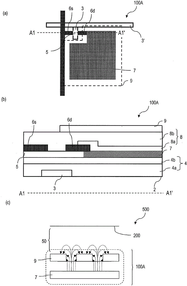
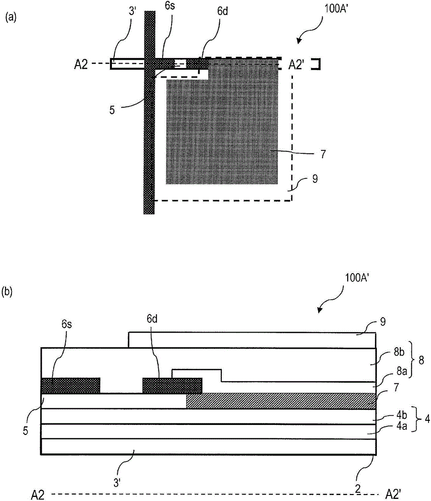
[0042] figure 1 (a) is a schematic plan view of TFT substrate 100A of this embodiment, figure 1 (b) is along figure 1 (a) A schematic cross-sectional view of a semiconductor device (TFT substrate) 100A along line A1-A1'. figure 1 (c) is a schematic ...


PUM


Abstract

A semiconductor device (100A) has: a substrate (2); an oxide semiconductor layer (5) formed on the substrate (2); a source electrode (6s) and a drain electrode (6d) which are electrically connected to the oxide semiconductor layer (5); a first transparent electrode (7) which is electrically connected to the drain electrode (6d); a dielectric layer (8) formed on the source electrode (6s) and the drain electrode (6d); and a second transparent electrode (9) formed on the dielectric layer (8). The upper surface and / or lower surface of the first transparent electrode (7) contact(s) a reducing / insulating layer (8a) having a property that reduces the oxide semiconductor included in the oxide semiconductor layer (5). At least part of the second transparent electrode (9) overlaps the first transparent electrode (7) with the dielectric layer (8) interposed therebetween. The oxide semiconductor layer (5) and the first transparent electrode (7) are formed from the same oxide film.

Description

technical field [0001] The present invention relates to a semiconductor device formed using an oxide semiconductor and a manufacturing method thereof, and more particularly to an active matrix substrate of a liquid crystal display device and an organic EL display device and a manufacturing method thereof. Here, the semiconductor device includes an active matrix substrate and a display device including the same. Background technique [0002] In an active matrix substrate used in a liquid crystal display device, a switching element such as a thin film transistor (Thin Film Transistor, hereinafter referred to as "TFT") is formed for each pixel. An active matrix substrate including TFTs as switching elements is called a TFT substrate. [0003] As TFTs, TFTs having an active layer of an amorphous silicon film (hereinafter referred to as "amorphous silicon TFT") and TFTs having a polysilicon film as an active layer (hereinafter referred to as "polysilicon TFT") have been widely u...

Claims


Application Information

Patent Timeline
Patent Type & Authority Applications(China)
IPC IPC(8): H01L21/336G09F9/00G09F9/30H01L27/32H01L29/786
CPCH01L27/3262H01L29/78606H01L29/7869H01L21/441H01L29/66969H01L27/127H01L29/4908H01L27/1225H10K59/1213
Inventor 宫本忠芳伊东一笃森重恭宫本光伸小川康行中泽淳内田诚一松尾拓哉
Owner SHARP KK
Why Eureka
Try Eureka