Semiconductor fingerprint identification sensor and manufacture method thereof

A fingerprint recognition and semiconductor technology, applied in the fields of semiconductor/solid-state device manufacturing, semiconductor devices, semiconductor/solid-state device components, etc., can solve the problems of high cost, low signal-to-noise ratio, poor reliability, etc., to reduce process costs, reduce Signal loss, the effect of simplifying the manufacturing process

Active Publication Date: 2014-10-15
BOE TECH GRP CO LTD
View PDF5 Cites 35 Cited by
  • Summary
  • Abstract
  • Description
  • Claims
  • Application Information

AI Technical Summary

Problems solved by technology

But its disadvantages are also obvious: the use of single crystal silicon as a Sensor (inductor) has high cost, low signal-to-noise ratio, poor reliability, etc.
Existing semiconductor fingerprint sensors use s

Method used


Image

  • Semiconductor fingerprint identification sensor and manufacture method thereof
  • Semiconductor fingerprint identification sensor and manufacture method thereof

Examples


Example Embodiment

[0035] The specific embodiments of the present invention will be described in further detail below in conjunction with the drawings and embodiments. The following examples are used to illustrate the present invention, but not to limit the scope of the present invention.

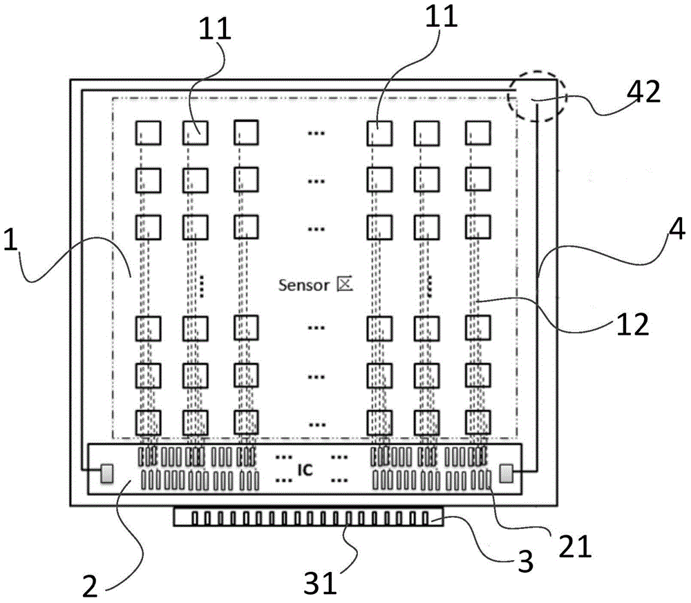
[0036] Such as figure 1 As shown, the present invention provides a semiconductor fingerprint recognition sensor, which includes a sensing area 1, a control area 2 and an interface area 3; the sensing area 1, the control area 2 and the interface area 3 are in communication connection; the fingerprint information sensed by the sensing area 1 is sent to The control area 2 is processed and output through the interface area 3.

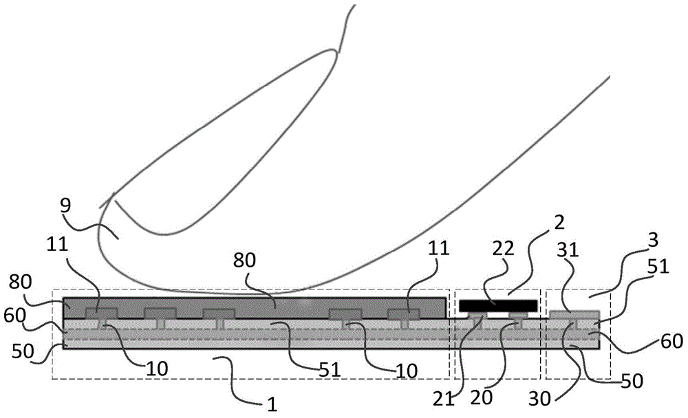
[0037] Such as figure 2 As shown, the sensing area 1 includes an insulating layer 50, a wiring layer 60, a substrate layer 51, and a protective layer 80 that are fixed in sequence. The wiring layer 60 is embedded between the insulating layer 50 and the substrate layer 51. A sensor array 11 i...


PUM


Abstract

The invention discloses a semiconductor fingerprint identification sensor and a manufacture method thereof. The semiconductor fingerprint identification sensor comprises an induction area, a control area and an interface area, wherein the induction area, the control area and the interface area are in communication connection; fingerprint information induced by the induction area is sent to the control area; after the fingerprint information is processed by the control area, the processed fingerprint information is output through the interface area; the induction area comprises an insulation layer, a routing layer, a substrate layer and a protection layer, wherein the insulation layer, the routing layer, the substrate layer and the protection layer are fixed in sequence; the routing layer is embedded between the insulation layer and the substrate layer; one surface, which contacts with the protection layer, on the substrate layer, is provided with sensor arrays; through holes corresponding to the sensor arrays are arranged on the substrate layer; and the sensor arrays are electrically connected with a sensing lead wire circuit of the routing layer through the through holes. The invention has the advantages of being low in cost, high in signal to noise ratio, high in reliability and simple in processing technology.

Description

Technical field [0001] The invention relates to a semiconductor fingerprint identification sensor and a manufacturing method thereof, belonging to the technical field of fingerprint identification. Background technique [0002] At present, the existing fingerprint recognition sensors mainly include optical fingerprint recognition sensors, surface acoustic wave fingerprint recognition sensors, and semiconductor fingerprint recognition sensors. [0003] The principle of the optical fingerprint recognition sensor is mainly the principle of optical photography and reflection. Its advantages are strong antistatic ability, low product cost, long service life, high dependence on light, inability to identify fake fingers, and poor applicability to wet and dry fingers And other shortcomings. [0004] The surface acoustic wave fingerprint recognition sensor has the disadvantages of large size and high power consumption. [0005] The semiconductor fingerprint sensor mainly uses the principles o...

Claims


Application Information

Patent Timeline
IPC IPC(8): G06K9/00
CPCH01L2224/16237H01L2924/15153H01L2924/15192H01L23/3121G06V40/1329G06V40/1306G06F18/00H01L21/486H01L23/49827H01L23/49838H01L23/4985H01L23/60H01L24/11H01L24/17H01L24/81H01L2224/11462H01L2224/16113H01L2224/16235H01L2224/81801
Inventor 逯家宁
Owner BOE TECH GRP CO LTD
Why Eureka
Try Eureka