
Low-cost microwave- and millimeter-wave polarized antenna of multi-layer PCB (Printed circuit board) process

A circularly polarized antenna, low-cost technology, applied in the direction of antenna, slot antenna, radiating element structure, etc., can solve the problems of narrow bandwidth, only 0.7%-7%, large size and weight of circularly polarized microstrip antenna , to achieve the effect of small structure size, easy processing, and widening of the axial ratio bandwidth

Inactive Publication Date: 2014-10-15
SOUTHEAST UNIV
View PDF4 Cites 62 Cited by
  • Summary
  • Abstract
  • Description
  • Claims
  • Application Information

AI Technical Summary

Problems solved by technology

[0004] Through the study of existing patents, the patent "Dual-band Wide Beam Circular Polarization Antenna with Good Low Elevation Angle Performance" discloses a dual-band monopole antenna, which is mainly composed of active inverted L-shaped monopole and The antenna is composed of a ground plane. This antenna does not belong to the microstrip antenna, and its size and weight are large.
While the circularly polarized microstrip antenna has a series of advantages, it also has some disadvantages. Due to its narrow bandwidth, the relative bandwidth of the circularly polarized microstrip antenna is generally only 0.7%-7%, so it has received certain attention in practical applications. limits

Method used


Image

  • Low-cost microwave- and millimeter-wave polarized antenna of multi-layer PCB (Printed circuit board) process
  • Low-cost microwave- and millimeter-wave polarized antenna of multi-layer PCB (Printed circuit board) process
  • Low-cost microwave- and millimeter-wave polarized antenna of multi-layer PCB (Printed circuit board) process

Examples


Embodiment Construction

[0025] The present invention will be further described below in conjunction with the accompanying drawings and specific embodiments.

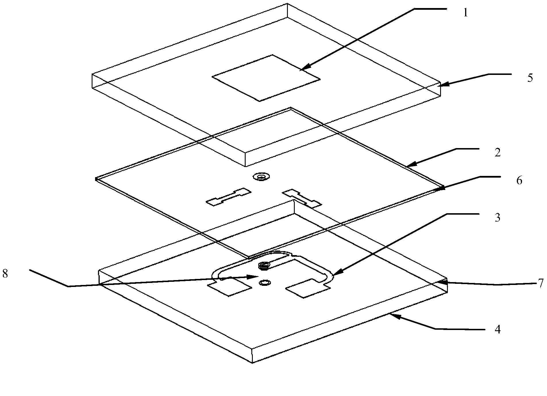
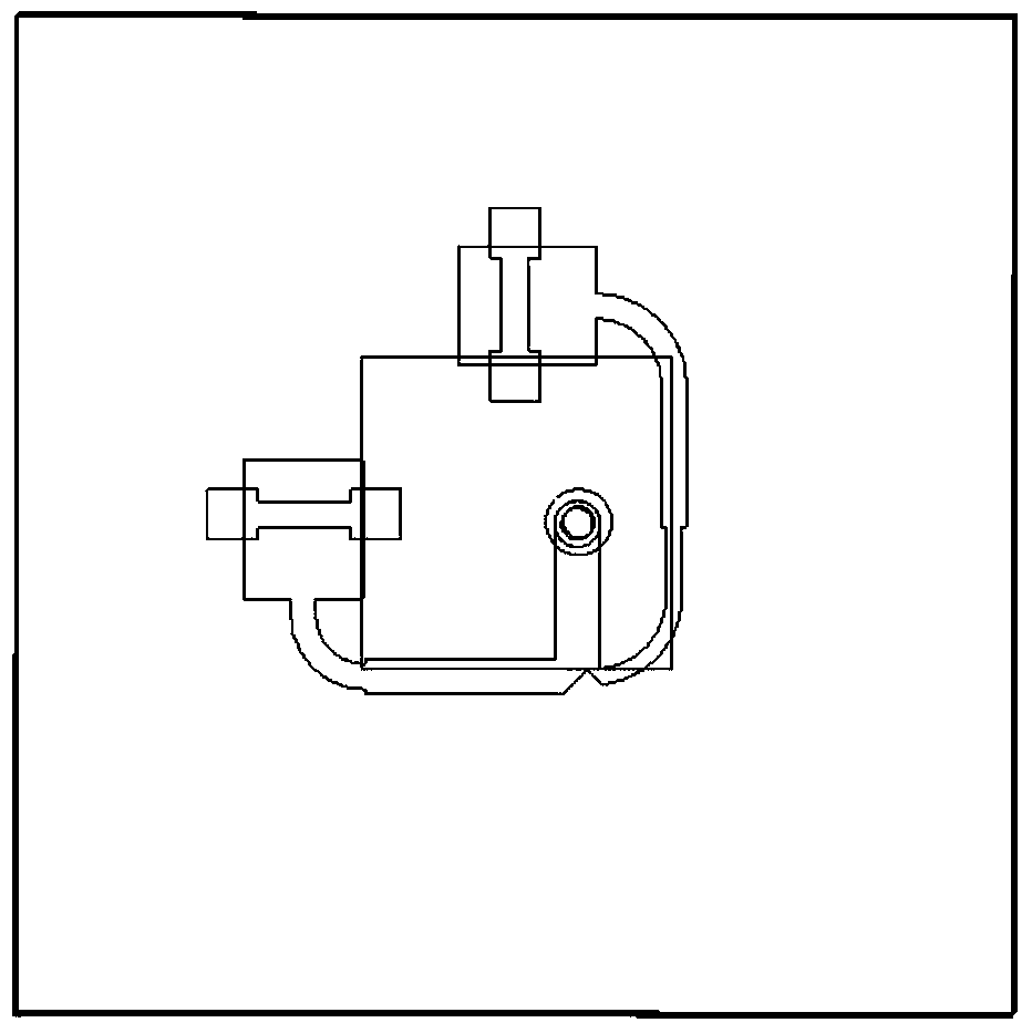
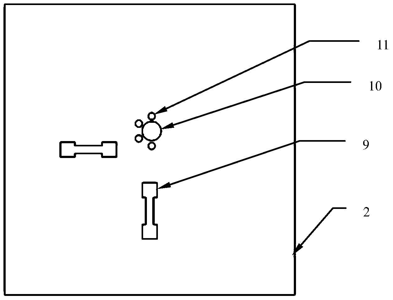
[0026] Such as figure 1 , 2 As shown, the specific multilayer structure of the low-cost microwave and millimeter wave circularly polarized antenna of the multilayer PCB process of the present invention is as follows, a square radiation metal patch 1 and an upper dielectric substrate 5, a metal floor 2 with an H-shaped coupling gap and The middle dielectric substrate 6 , the feed metal plate 3 with a power distribution network, the lower dielectric substrate 7 , and the bottom metal floor 4 . It also includes the grounding metal through hole connecting the metal floor 2 with the H-shaped coupling gap and the bottom metal floor 4, and the coaxial connection between the feed metal plate 3 with the power dividing network and the feed input port on the bottom metal floor 4. Microstrip Transition Structure8.

[0027] The radiation metal patch 1 is...


PUM


Abstract

The invention discloses a low-cost microwave- and millimeter-wave polarized antenna of the multi-layer PCB (Printed circuit board) process. The polarized antenna is of a multi-layer structure and comprises a quadrate radiating metal patch, an upper dielectric substrate, a metal floor equipped with an H-shaped coupling gap, a medium dielectric substrate, a feed metal plate with power division network, a lower dielectric substrate and a bottom metal floor; the quadrate radiating metal patch is coupled with the floor equipped with the H-shaped coupling gap to realize feed; the feed network of a microstrip line structure is positioned below the floor; the metal floor equipped with the H-shaped coupling gap is connected with the bottom metal floor through a metal through hole; the feed metal plate with the power division network is connected with the bottom metal floor through a second metal through hole to form a coaxial microstrip line conversion structure by which feeding from the bottom part of the antenna is realized. The antenna has the characteristics that the frequency band is wide, the size is small, the cost is low, the manufacturing and processing are simple, and the axial ratio feature is great.

Description

technical field [0001] The invention belongs to the field of circularly polarized antennas, and in particular relates to a low-cost circularly polarized antenna with a multilayer PCB (printed circuit board) process in the microwave and millimeter wave bands. Background technique [0002] With the development of wireless communication technology, it is difficult for an antenna with a single polarization mode to meet the requirements. Especially in the field of satellite communication, there are usually requirements for antenna polarization characteristics, size, and weight. Circularly polarized antennas can receive incoming waves of any polarization, and their radiated waves can also be received by antennas of any polarization, which can suppress rain and fog interference and anti-multipath reflection, so they are widely used in the field of satellite communications. [0003] Circularly polarized antennas can be implemented in a variety of ways, and can be divided into micros...

Claims


Application Information

Patent Timeline
IPC IPC(8): H01Q13/10H01Q13/08H01Q1/36
Inventor 陈鹏周圆余旭涛张慧刘明阳曾绍祥蔡晓菲施丽慧
Owner SOUTHEAST UNIV
Learn More