Light-emitting diode packaging structure

A technology of light-emitting diodes and packaging structures, applied in electrical components, electrical solid-state devices, circuits, etc., can solve the problems of low excitation efficiency and weak luminous intensity of phosphors

Inactive Publication Date: 2014-10-29
ZHANJING TECH SHENZHEN +1
View PDF4 Cites 5 Cited by
  • Summary
  • Abstract
  • Description
  • Claims
  • Application Information

AI Technical Summary

Problems solved by technology

Since the light emitted by the light-emitting diode chip is concentrated from its top side to excite the phosphor powder in the upper area of ​​the reflective cup, while the light emitted from the periphery of the light-emitting diode chip is less and the luminous intensity is weaker, so it cannot or only a small part Excitation of the phosphor deposited in the bottom area of ​​the reflector cup, resulting in a lower overall excitation efficiency of the phosphor

Method used


Image

  • Light-emitting diode packaging structure
  • Light-emitting diode packaging structure

Examples


Embodiment Construction

[0012] The present invention will be further described in detail below in conjunction with the accompanying drawings.

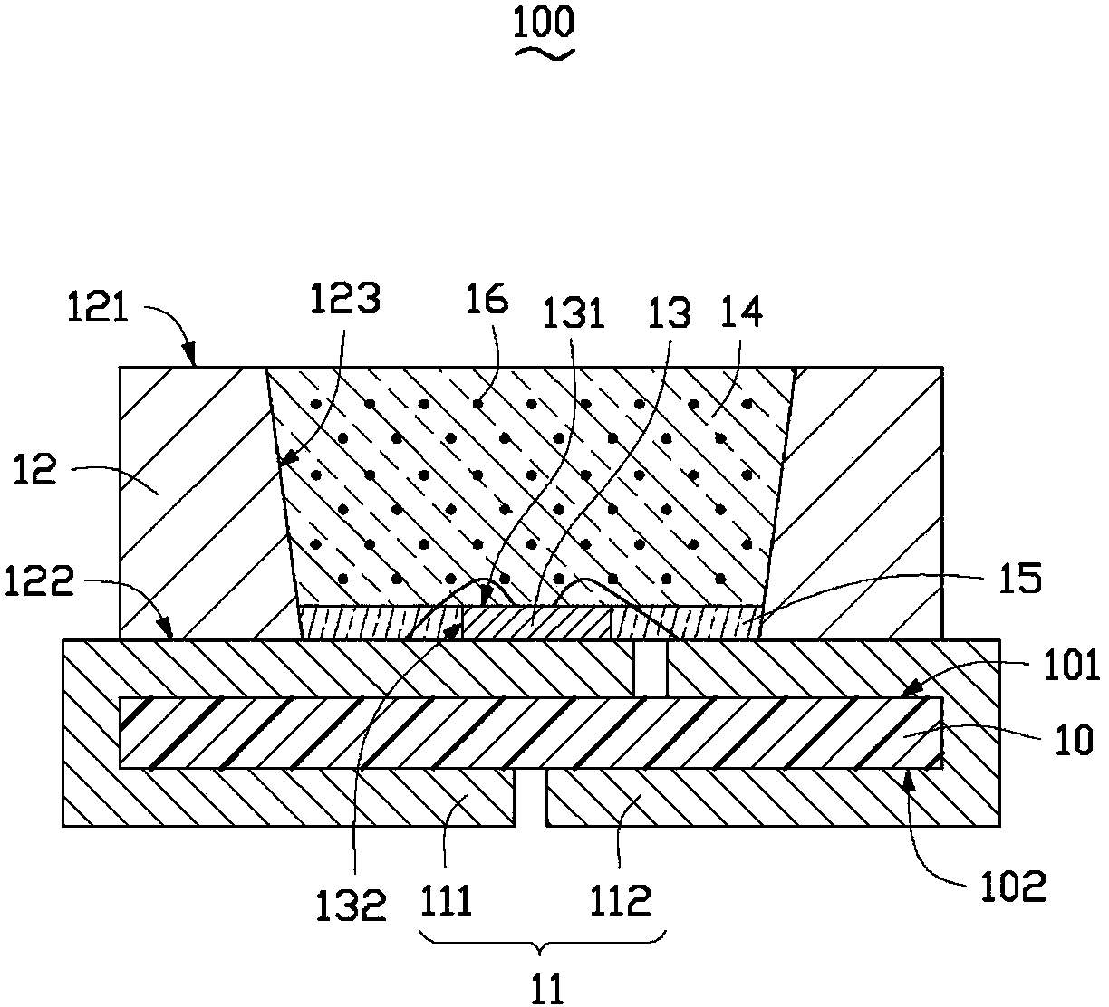
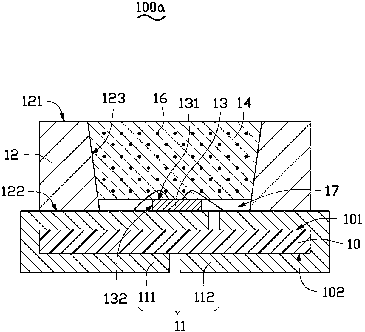
[0013] Such as figure 1 As shown, a light emitting diode packaging structure 100 provided for a preferred embodiment of the present invention includes a substrate 10, a lead structure 11 disposed on the substrate 10, a light emitting diode chip 13 disposed on the lead structure 11, a first An encapsulation layer 14 and a second encapsulation layer 15 , and a reflection cup 12 formed on the substrate 10 and containing the LED chip 13 .

[0014] Specifically, the substrate 10 is flat and includes a first surface 101 and a second surface 102 opposite to the first surface 101 . In this embodiment, the substrate 10 is an insulating substrate.

[0015] The pin structure 11 extends from the first surface 101 to the second surface 102 . The pin structure 11 includes a first electrode 111 and a second electrode 112 spaced apart from each other. The first electrode...


PUM


Abstract

A light emitting diode (LED) package includes a substrate, a pin structure and a reflector formed on the substrate, an LED chip arranged on the pin structure and a first encapsulation layer mixed with phosphor filled in the reflector. The LED chip includes a top surface, a side surface extending downward from the top surface and a bottom surface opposite to the top surface. A bottom end of the first encapsulation layer is located above the top surface of the LED chip. A transparent second encapsulation layer is located below the first encapsulation layer and surrounds the LED die.

Description

technical field [0001] The invention relates to a semiconductor structure, in particular to a light emitting diode packaging structure. Background technique [0002] A light emitting diode (Light Emitting Diode, LED) is a semiconductor element that can convert electric current into light in a specific wavelength range. Light-emitting diodes can be widely used as light sources in the field of lighting because of their advantages such as high brightness, low operating voltage, low power consumption, easy matching with integrated circuits, simple driving, and long life. [0003] The existing LED packaging structure generally includes a LED chip, a reflective cup for containing the LED chip, and a packaging layer filled in the reflective cup, covering the LED chip and mixed with phosphor powder. The light emitted by the LED chip excites the The phosphor powder in the encapsulation layer mixes to form white light and then emits it. Since the light emitted by the light-emitting ...

Claims


Application Information

Patent Timeline
Patent Type & Authority Applications(China)
IPC IPC(8): H01L33/54H01L33/50
CPCH01L33/52H01L33/60H01L33/508H01L33/54H01L33/56H01L2224/48091H01L2224/48247H01L2924/00014
Inventor 黄哲瑄林新强叶辅湘
Owner ZHANJING TECH SHENZHEN
Why Eureka
Try Eureka