OLED phase inverting circuit and display panel

An inverter circuit and panel technology, applied in the field of OLED display, can solve the problems of insufficient high and low potential, inability to effectively control TFT, and inability of compensation circuit to work effectively.

Active Publication Date: 2014-11-05
WUHAN TIANMA MICRO ELECTRONICS CO LTD +1
View PDF5 Cites 12 Cited by
  • Summary
  • Abstract
  • Description
  • Claims
  • Application Information

AI Technical Summary

Problems solved by technology

But in the above circuit, OUT is connected to VGH and VGL at the same time. If the on/off of TFT is complete, then OUT will only be connected to VGH or VGL. The output voltage of OUT must be VGH as high voltage and VGL as low voltage. However, the above circuit has the problem that two TFTs are turned on at the same time. Because of the effect of voltage division, the output voltage of OUT is the intermediate potential of the two,

Method used


Image

  • OLED phase inverting circuit and display panel
  • OLED phase inverting circuit and display panel
  • OLED phase inverting circuit and display panel

Examples


Embodiment Construction

[0030] The following will clearly and completely describe the technical solutions in the embodiments of the present invention with reference to the accompanying drawings in the embodiments of the present invention. Obviously, the described embodiments are only some, not all, embodiments of the present invention. Based on the embodiments of the present invention, all other embodiments obtained by persons of ordinary skill in the art without creative efforts fall within the protection scope of the present invention.

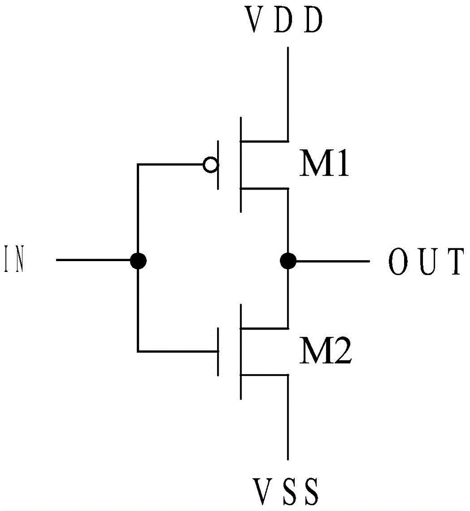
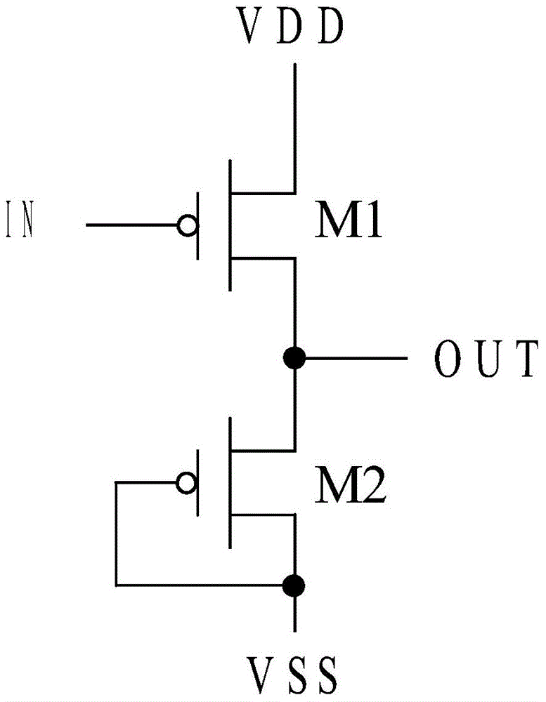
[0031] Such as Figure 3a Shown is a structural diagram of an inverting circuit provided by an embodiment of the present invention, including: a first transistor M1, a second transistor M2, a third transistor M3, a fourth transistor M4 and a first capacitor C1, all of the above transistors are P-type transistors.

[0032] Wherein, the first pole of the first transistor M1 is connected to the second terminal of the first capacitor C1 and the third pole of the third...


PUM


Abstract

The invention discloses a phase inverting circuit and a driving method thereof and is characterized in that the phase inverting circuit includes a pull-up unit which is provided with a first power supply input end, a first end, a second end and a third end, wherein the first power supply input end receives a first power supply voltage, the first end receives a first control signal and the third end is electrically connected with a signal output end and outputs a first level signal; a pull-down unit which is provided with a second power supply input end, a forth end, a fifth end and a sixth end, wherein the forth end is electrically connected with the second end of the pull-up unit, the second power supply input end receives a second power supply voltage, the fifth end receives a second control signal and the sixth end is electrically connected with the signal output end and outputs a second level signal; and a first capacitor, wherein a first end of the first capacitor is electrically connected with the second end of the pull-up unit and the forth end of the pull-down unit, and a second end of the first capacitor is electrically connected with the third end of the pull-up unit and the sixth end of the pull-down unit.

Description

technical field [0001] The invention relates to the technical field of OLED display, in particular to an OLED inverting circuit and a display panel. Background technique [0002] In recent years, in the field of display devices that display images, optical devices using current-driven types whose luminous brightness changes according to the value of the flowing current, for example, organic electroluminescent devices (OLEDs) have been developed as light-emitting devices of pixels The display device of the device. Unlike a liquid crystal device or the like, an OLED is a self-luminous device, and in a display device using an OLED, gradation of coloring is achieved by controlling a current value in the OLED. [0003] Like liquid crystal displays, there are passive matrix systems and active matrix systems in the driving systems of OLED display devices. The former is simple in structure, but has disadvantages such as difficulty in realizing a large and high-resolution display d...

Claims


Application Information

Patent Timeline
IPC IPC(8): G09G3/32G09G3/3258H05B44/00
CPCG09G2310/0289G09G3/3225G09G3/3677G09G3/3266G09G2310/0286H05B45/60
Inventor 吴桐钱栋
Owner WUHAN TIANMA MICRO ELECTRONICS CO LTD
Why Eureka
Try Eureka