Semitransparent photoconversion device
A light conversion and device technology, applied in the manufacturing of semiconductor devices, optical components, semiconductor/solid-state devices, etc., can solve the problems of lack of thickness control of insulating layer, no direct effect of solar cell device performance, etc.
- Summary
- Abstract
- Description
- Claims
- Application Information
AI Technical Summary
Problems solved by technology
Method used
Image

Examples
Embodiment Construction
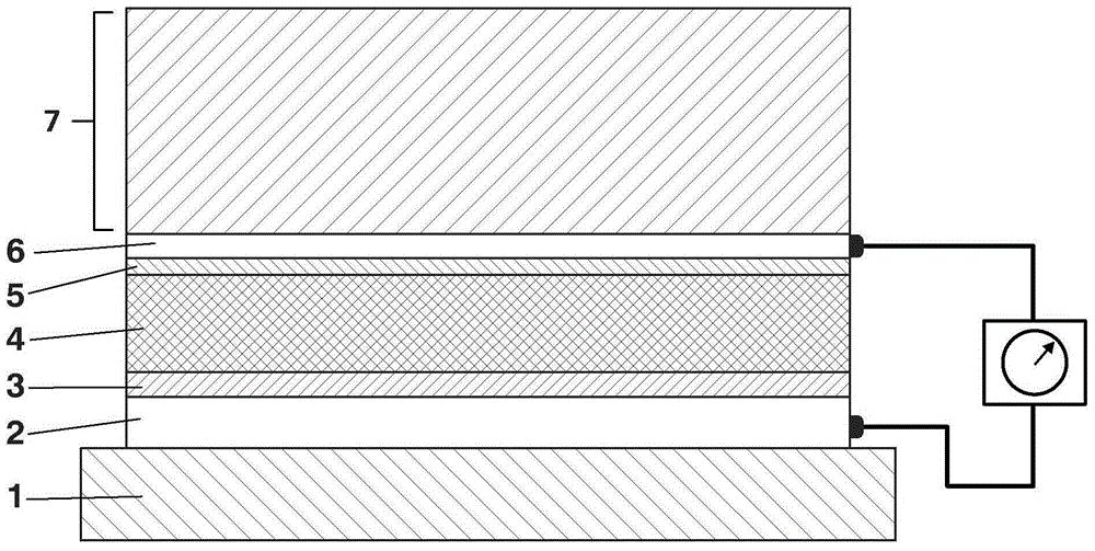
[0021] The light conversion device has a direct or reverse structure, including a first light-transmitting electrical contact covering a transparent substrate, a charge blocking layer covering the first light-transmitting electrical contact and located below an active organic photosensitive material, and a second layer covering the active organic photosensitive material. Two charge blocking layers, a second light-transmitting electrical contact covering the second charge blocking layer, and a multilayer structure covering the second light-transmitting electrical contact. Multilayer structures consist of more than two layers of dielectric materials. In such multilayer structures, the refractive index of each layer must be different from that of adjacent layers. The method of manufacturing a photovoltaic cell comprising said multilayer structure comprises one deposition step for each layer in said device. The fabrication of the entire device ends with the deposition of the last...
PUM
 Abstract
Description
Claims
Application Information
 - R&D
- Intellectual Property
- Life Sciences
- Materials
- Tech Scout
- Unparalleled Data Quality
- Higher Quality Content
- 60% Fewer Hallucinations
Browse by: Latest US Patents, China's latest patents, Technical Efficacy Thesaurus, Application Domain, Technology Topic, Popular Technical Reports.
© 2025 PatSnap. All rights reserved.Legal|Privacy policy|Modern Slavery Act Transparency Statement|Sitemap|About US| Contact US: help@patsnap.com