Supercharge Your Innovation With Domain-Expert AI Agents!

Manufacture method of control gate and manufacture method of floating gate

A manufacturing method and control gate technology, applied in semiconductor/solid-state device manufacturing, electrical components, semiconductor devices, etc., can solve the problems of small size, damage, and lower semiconductor wafer yield, so as to improve yield and avoid damage Effect

Inactive Publication Date: 2014-11-19
SEMICON MFG INT (SHANGHAI) CORP
View PDF8 Cites 6 Cited by
  • Summary
  • Abstract
  • Description
  • Claims
  • Application Information

AI Technical Summary

Problems solved by technology

[0006] However, as the feature size of the semiconductor industry continues to decrease, in the process of making the control gate of flash memory, the shape and size of the control gate will have a great impact on the yield of flash memory
Since the material of the floating gate layer 20 and the control gate layer 40 is polysilicon, when the floating gate layer 20 is etched to form the floating gate 21, the sidewall of the control gate 41 will also be etched. etch, causing damage to the sidewall of the control gate 41, making the size of the control gate 41 smaller than the size required by the process, resulting in the surface morphology of the control gate 41 not meeting the process requirements, affecting the control gate 41. The size of the line resistance of 41 will also cause the subsequent connection lines formed on the control gate 41 to fail to form good contact with the control gate 41, thereby reducing the yield of the semiconductor wafer.

Method used


Image

  • Manufacture method of control gate and manufacture method of floating gate
  • Manufacture method of control gate and manufacture method of floating gate
  • Manufacture method of control gate and manufacture method of floating gate

Examples


Embodiment Construction

[0029] The manufacturing method of the control gate and the floating gate proposed by the present invention will be further described in detail below with reference to the drawings and specific embodiments. Advantages and features of the present invention will be apparent from the following description and claims. It should be noted that all the drawings are in a very simplified form and use imprecise scales, and are only used to facilitate and clearly assist the purpose of illustrating the embodiments of the present invention.

[0030] Please refer to figure 2 In this embodiment, a method for manufacturing a control gate and a floating gate is proposed, including the following steps:

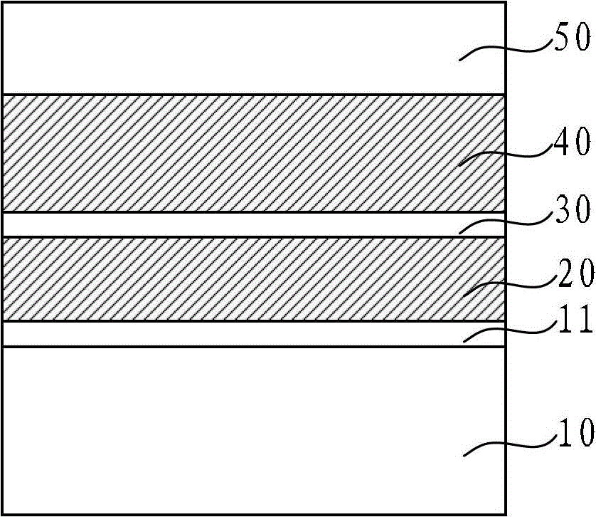
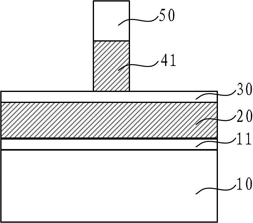
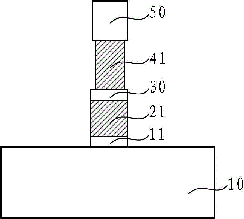
[0031] S100: providing a semiconductor substrate 100, where the semiconductor substrate 100 is a silicon substrate;

[0032] like Figure 3a As shown, shallow trench isolation (not shown) can be provided in the semiconductor substrate 100, and the material of the semiconductor substrate 100...


PUM


Abstract

The invention brings forward a manufacture method of a control gate. After the control gate is formed and before a floating gate layer is etched, preprocessing is performed on the control gate firstly, and then a dielectric layer, the floating gate layer and the gate medium layer are etched. Since the preprocessing is performed on the control gate, a protective layer is formed on the surface of the control gate for protecting the control gate so as to prevent damage caused to the surface of the control gate by etching, and the yield rate of a semiconductor wafer is improved.

Description

technical field [0001] The invention relates to the field of semiconductor manufacturing, in particular to a method for manufacturing a control gate and a floating gate. Background technique [0002] Memory is used to store large amounts of digital information. Currently there are many types of memory, such as RAM (random access memory), DRAM (dynamic random access memory), ROM (read-only memory), EPROM (erasable programmable read-only memory), FLASH (flash memory) and so on. [0003] Since the first flash memory product came out in the 1980s, with the development of technology and the storage needs of various electronic products, flash memory has been widely used in mobile and communication devices such as mobile phones, notebooks, handheld computers, and USB flash drives. , flash memory is a kind of non-volatile memory. Its operating principle is to control the switch of the gate channel by changing the critical voltage of the transistor or memory cell to achieve the purp...

Claims


Application Information

Patent Timeline
Patent Type & Authority Applications(China)
IPC IPC(8): H01L21/28H01L21/3213H01L21/311
CPCH01L29/42324H01L29/401
Inventor 何其暘尚飞
Owner SEMICON MFG INT (SHANGHAI) CORP
Features
  • R&D
  • Intellectual Property
  • Life Sciences
  • Materials
  • Tech Scout
  • Unparalleled Data Quality
  • Higher Quality Content
  • 60% Fewer Hallucinations
Learn More