LED epitaxial layer structure, LED epitaxial layer growing method and LED chip with LED epitaxial layer structure

A technology of LED chip and growth method, which is applied in the direction of electrical components, circuits, semiconductor devices, etc., can solve the problem that the brightness cannot be further improved, and achieve the effects of improving recombination efficiency, increasing overlap integral, and increasing the number

Active Publication Date: 2014-11-19
XIANGNENG HUALEI OPTOELECTRONICS
View PDF8 Cites 2 Cited by
  • Summary
  • Abstract
  • Description
  • Claims
  • Application Information

AI Technical Summary

Problems solved by technology

[0004] The purpose of the present invention is to provide an LED epitaxial layer structure and growth method to solve the technical problem that the brightness cannot be further improved in the prior art when the voltage of the LED chip remains unchanged.

Method used


Image

  • LED epitaxial layer structure, LED epitaxial layer growing method and LED chip with LED epitaxial layer structure
  • LED epitaxial layer structure, LED epitaxial layer growing method and LED chip with LED epitaxial layer structure
  • LED epitaxial layer structure, LED epitaxial layer growing method and LED chip with LED epitaxial layer structure

Examples


Embodiment 1

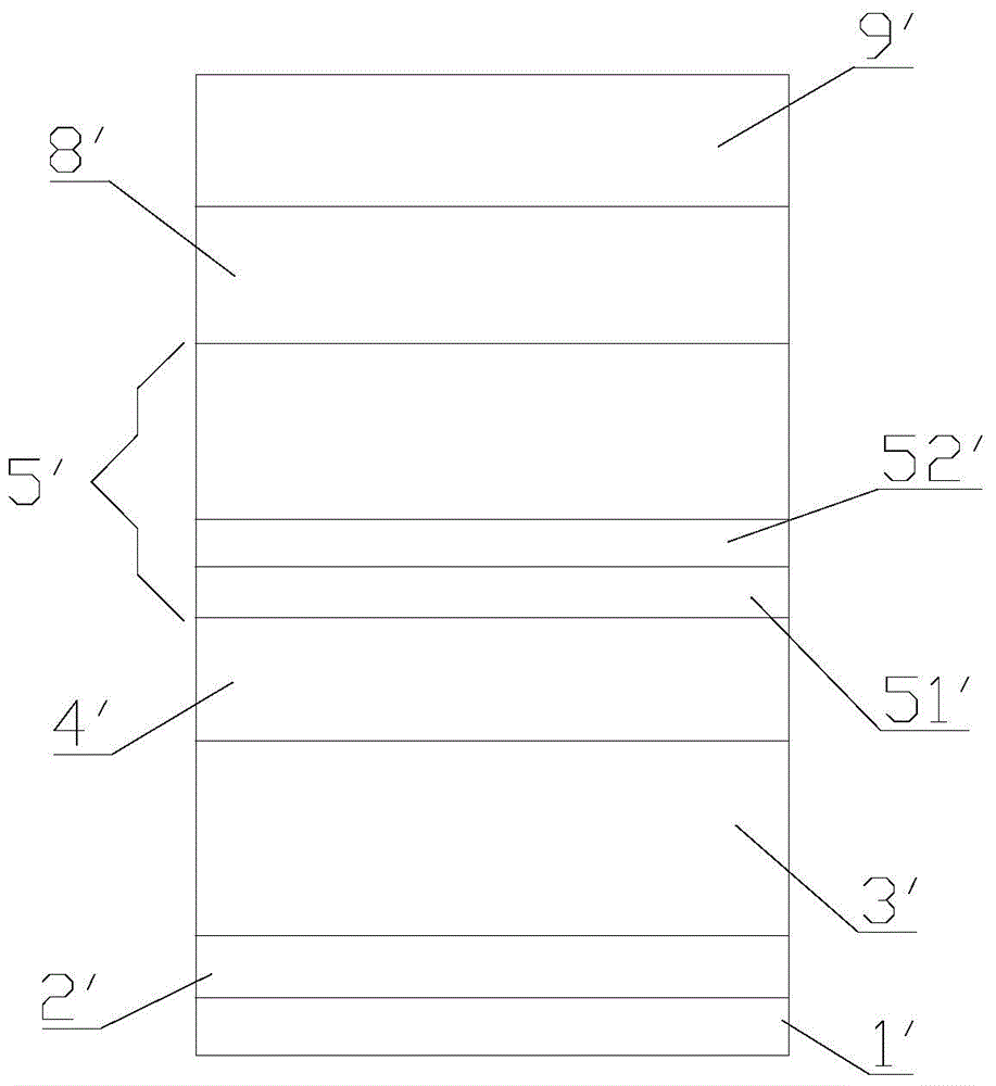
[0048] 1. Treat the sapphire substrate in a hydrogen atmosphere at 1000°C for 3 minutes;

[0049] 2. Cool down to 530°C and grow a GaN buffer layer with a thickness of 20nm on the sapphire substrate;

[0050] 3. Continue to grow 3um undoped GaN at a temperature of 1000°C;

[0051] 4. Then first grow 3μm N-type GaN continuously doped with Si, and the Si doping concentration is 1E+19;

[0052] 5. The light-emitting layer MQW is periodically grown, and the number of MQW unit cycles is 14, and the In in each cycle x Ga (1-x) The N layer is grown at 700°C and doped with In, with a thickness of 2.5nm. In the MQW unit x Ga (1-x) N (where x starts from the first In x Ga (1-x) 0.05 uniform gradient of N layer to 14th In x Ga (1-x) 0.3 of the N layer, the gradient rate is 0.017 / cycle) layer, the growth temperature of each GaN layer is 800°C, and the thickness is 11nm.

[0053] 6. Then raise the temperature to 900°C and continue to grow a 20nm P-type AlGaN layer with an Al dopi...

Embodiment 2

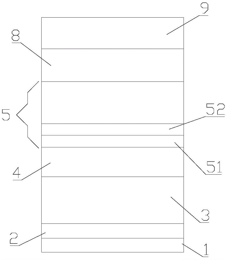
[0057] 1. Treat the sapphire substrate in a hydrogen atmosphere at 1200°C for 5 minutes;

[0058] 2. Cool down to 560°C and grow a buffer layer GaN with a thickness of 30nm on the sapphire substrate;

[0059] 3. Raise the temperature to 1100°C and continue to grow 4um undoped GaN;

[0060] 4. Then first grow 4μm N-type GaN continuously doped with Si, and the Si doping concentration is 2E+19;

[0061] 5. The light-emitting layer MQW is periodically grown, and the number of MQW unit periods is 16. Each In in the MQW unit x Ga (1-x) The N layers are all grown at 750°C doped with In, and each layer of In x Ga (1-x) The thickness of the N layer is 3 nm. In the MQW unit x is determined by the first In x Ga (1-x) The 0.30 uniform gradient of the N layer to the 16th In x Ga (1-x) 0.05 in the N layer, the gradual change rate is 0.017 / cycle), and the growth temperature of each GaN layer is 850°C, and the growth thickness is 12nm;

[0062] 6. Then raise the temperature to 930°...

Embodiment 3

[0066] 1. Treat the sapphire substrate in a hydrogen atmosphere at 1100°C for 4 minutes;

[0067] 2. Cool down to 550°C and grow a GaN buffer layer with a thickness of 25nm on the sapphire substrate;

[0068] 3. Raise the temperature to 1150°C and continue to grow 3.5um undoped GaN;

[0069] 4. Then first grow 3.5μm N-type GaN continuously doped with Si, and the Si doping concentration is 1.5E+19;

[0070] 5. The light-emitting layer MQW is periodically grown, and the number of MQW unit periods is 15. Each In in the MQW unit x Ga (1-x) The N layers are all grown at 740°C and doped with In. Each layer In x Ga (1-x) The thickness of the N layer is 2.5 nm. In the MQW unit x is determined by the first In x Ga (1-x) 0.1 uniform gradient of N to the 15th In x Ga (1-x) 0.3 in the N layer, the gradient rate is 0.013 / cycle) layer, the growth temperature of each GaN layer: 840°C, and the thickness is 11nm. ;

[0071] 6. Then raise the temperature to 920°C and continue to gr...


PUM


Abstract

The invention provides an LED epitaxial layer structure, an LED epitaxial layer growing method and an LED chip with the LED epitaxial layer structure. The LED epitaxial layer structure comprises a Si-N mingled type GaN layer, an MQW layer and a P type AlGaN layer, which are all overlapped in sequence, wherein the MQW layer comprises a plurality of MQW units sequentially arranged in an overlapping manner; each MQW unit comprises InXGa (1-X) N layers and GaN layers, which are arranged in an overlapping manner; the Xs of the InXGa (1-X) N layers ramp from 0.05-0.3 to 0.3-0.05 at a constant speed in the direction from the Si-N mingled type GaN layer to the P type AlGaN layer. The LED chip provided by the invention has the advantages that In components ramp firstly, and the quasi-quantum dots of the luminous layer can be increased through adjusting the distribution fluctuation of the In components in multiple quantum well layers, so as to improve the overlapping integration of electrons and the hole wave function and enhance the composite efficiency of the electrons and the hole.

Description

technical field [0001] The invention relates to the field of LED (Light Emitting Diode), in particular to an LED epitaxial layer structure, a growth method and an LED chip with the structure. Background technique [0002] In the LED market, the driving voltage of LED chips is now required to be low, especially under high current, the smaller the driving voltage, the better, and the higher the light efficiency, the better; the LED market value is reflected in (light effect) / unit price, the better the light effect, the higher the price High, so LED high light efficiency has always been the goal pursued by LED manufacturers and LED research institutes in colleges and universities. see figure 1 The LED epitaxial layer structure used in the prior art includes a substrate 1' and a buffer GaN layer 2', a U-type GaN layer 3', and a Si-N-doped GaN layer 4' stacked on the top surface of the substrate 1' in sequence. , MQW layer 5', P-type AlGaN layer 8', magnesium-doped P-type GaN l...

Claims


Application Information

Patent Timeline
Patent Type & Authority Applications(China)
IPC IPC(8): H01L33/00H01L33/06
CPCH01L33/007H01L33/06H01L33/32
Inventor 林传强戚运东周佐华
Owner XIANGNENG HUALEI OPTOELECTRONICS
Why Eureka
Try Eureka