Air gap forming method in back-end-of-line process

An air gap and process technology, applied in the direction of electrical components, semiconductor/solid-state device manufacturing, circuits, etc., can solve the problem of damage to the through-hole structure, achieve the effect of reducing the K value and avoiding damage

Active Publication Date: 2014-11-26
SHANGHAI INTEGRATED CIRCUIT RES & DEV CENT
View PDF4 Cites 2 Cited by
  • Summary
  • Abstract
  • Description
  • Claims
  • Application Information

AI Technical Summary

Problems solved by technology

[0012] Here, in the process of removing the oxide-like film material, dilute HF (DHF) is usually used for wet etching. However, actual experiments have confirmed that the etching rate of DHF for the low-K dielectric material BDII is greater than that of the oxide-like film. rate, so that in the process of forming the air gap, other parts of the low-K dielectric material BDII will also be etched away, or even all of the BDII will be etched away, such as Figure 8 As shown, the top of the low-K dielectric layer and the part adjacent to the sidewall of the via structure are etched away, seriously damaging the via structure

Method used


Image

  • Air gap forming method in back-end-of-line process
  • Air gap forming method in back-end-of-line process
  • Air gap forming method in back-end-of-line process

Examples


Embodiment Construction

[0038] In order to make the content of the present invention clearer and easier to understand, the content of the present invention will be further described below in conjunction with the accompanying drawings. Of course, the present invention is not limited to this specific embodiment, and general replacements known to those skilled in the art are also covered within the protection scope of the present invention.

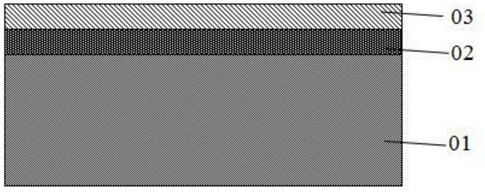
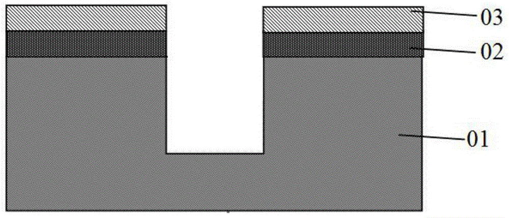
[0039] As mentioned above, usually when the air gap is prepared in the low-K dielectric layer, other parts of the low-K dielectric layer will be corroded, seriously damaging the through-hole structure; for this reason, the present invention provides an air gap formation The method is applied in the subsequent interconnection process, by thinning the hard mask layer and etching away the hard mask layer located on the top of the oxide-like film material, thereby exposing the oxide-like film material so as to remove the Oxide film: due to the protection of the hard ma...


PUM


Abstract

The invention provides an air gap forming method in the back-end-of-line process. The method includes the steps that a semiconductor substrate with a back-end-of-line film layer structure is provided; the back-end-of-line film layer structure is sequentially provided with a low-K dielectric layer and a hard mask layer from bottom to top; a through hole structure is respectively etched in the low-K dielectric layer and the hard mask layer through a photoetching process and an etching process; the side wall of the through hole structure in the low-K dielectric layer is modified through etching so as to form class oxidation film type material; the through hole structures are deposited with seed crystal layers and filled with metal copper; the top of the filling metal copper is subjected to planarization; the hard mask layer is subjected to downward reduction; the hard mask layer located at the top of the oxidation film type material is removed, and the top of the oxidation film type material is exposed outside; the oxidation film type material is removed, and the hard mask layer on which reduction has been conducted is removed, so that in the process of removing the oxidation film type material, the low-K dielectric layer is not damaged, damage to the through hole structures is avoided, and the K value of devices prepared in the later processes is further reduced.

Description

technical field [0001] The invention relates to the technical field of semiconductors, in particular to a method for forming an air gap in a subsequent interconnection process. Background technique [0002] With the continuous development and progress of integrated circuit technology, the critical dimensions of semiconductor manufacturing processes continue to shrink, and the cross-sectional area and distance between interconnect lines on the chip continue to decrease, which leads to the increase of interconnect resistance R and parasitic capacitance C, and the increased interconnection The connection resistance R and the parasitic capacitance C greatly increase the time constant RC of the interconnection. Therefore, the time constant RC of the interconnection line has an increasing influence on the delay of the integrated circuit, which becomes the main reason for limiting the interconnection speed. Above 0.13um process, semiconductors usually use aluminum as the metal mat...

Claims


Application Information

Patent Timeline
IPC IPC(8): H01L21/768
CPCH01L21/7682
Inventor 姚嫦娲胡正军林宏王伟军黄仁东
Owner SHANGHAI INTEGRATED CIRCUIT RES & DEV CENT
Why Eureka
Try Eureka