OLED panel and manufacturing method thereof

A manufacturing method and panel technology, applied in semiconductor/solid-state device manufacturing, electrical components, electrical solid-state devices, etc., can solve problems such as increasing power consumption, mask collapse, affecting driving voltage, etc., to prevent evaporation pattern deformation, reduce Small driving voltage, the effect of preventing lateral diffusion

Active Publication Date: 2017-02-15
EVERDISPLAY OPTRONICS (SHANGHAI) CO LTD
View PDF4 Cites 0 Cited by
  • Summary
  • Abstract
  • Description
  • Claims
  • Application Information

AI Technical Summary

Problems solved by technology

In order to ensure that the cathode resistance will not be too large, which will affect the driving voltage and increase power consumption, the size, area and distribution of the photosensitive gap body have certain restrictions.
However, the small number of photosensitive spacers will lead to insufficient support for the mask, and the mask may collapse locally, making the mask and the substrate not parallel, resulting in shifting of the coating position, which may seriously cause color mixing.

Method used


Image

  • OLED panel and manufacturing method thereof
  • OLED panel and manufacturing method thereof
  • OLED panel and manufacturing method thereof

Examples


Embodiment Construction

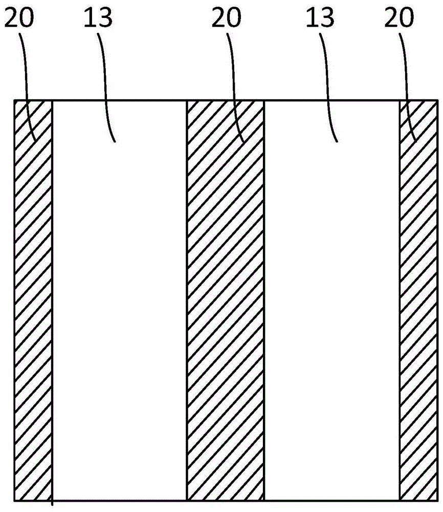
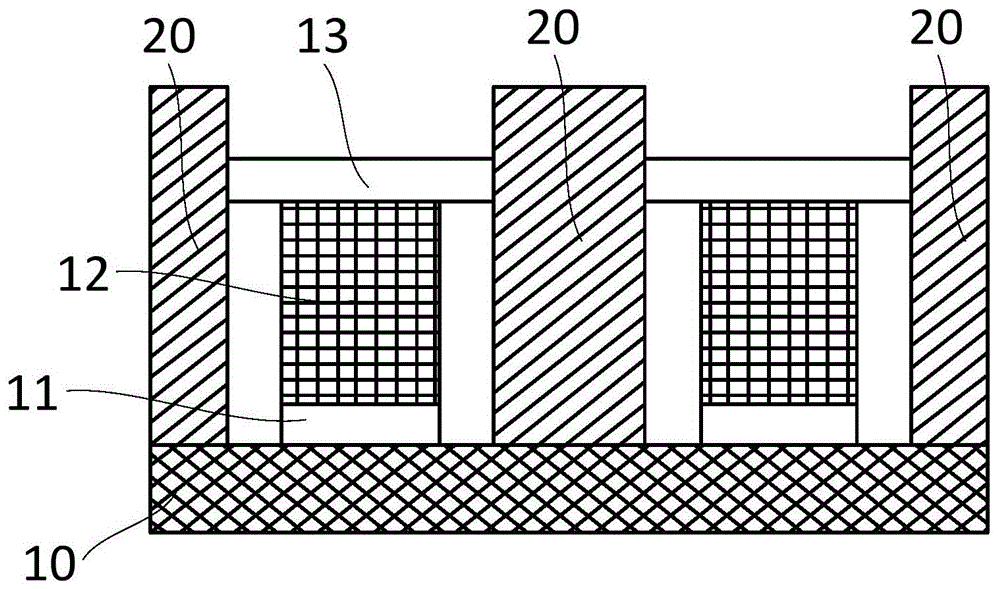
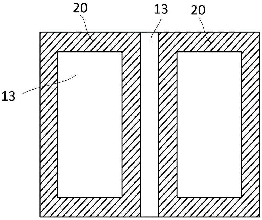
[0027] In order to prevent color mixing between adjacent pixels during the evaporation process of organic light-emitting materials, a layer of photosensitive spacer between the mask and the substrate is usually arranged on the substrate, and its function is to support the mask and prevent the mask from directly contacting the substrate. . The position of the photosensitive spacer is generally close to a single pixel area, and the photosensitive spacer is generally an insulator. In order to ensure that the cathode resistance will not be too large, which will affect the driving voltage and increase power consumption, the size, area and distribution quantity of the photosensitive spacers are limited to a certain extent. However, the small number of photosensitive spacers will lead to insufficient support for the mask, and the mask may partially collapse, making the mask and the substrate not parallel, resulting in shifting of the coating position, which may seriously cause color ...


PUM


Abstract

The invention discloses an OLED panel and a manufacturing method thereof. The OLED panel includes: a substrate having an insulating surface; a plurality of first pixel electrodes located on the surface of the substrate; conductive photosensitive gap bodies located on the surface of the substrate and between adjacent first pixel electrodes; and organic luminescent layers located on the first pixel electrodes. In the technical scheme of the invention, the conductive photosensitive gap bodies are adopted, influence of the photosensitive gap bodies on an OLED cathode resistance can be reduced under the circumstance of a large increase in the number of the photosensitive gap bodies, on the one hand, the adoption of the conductive photosensitive gap bodies can reduce resistance of the OLED cathode, and on the other hand, due to a barrier effect of the photosensitive gap bodies, the photosensitive gap bodies can effectively prevent transverse diffusion of vapor deposition material in a vapor deposition process, thereby effectively solving the problem of color mixing among different pixels of the OLED panel.

Description

technical field [0001] The invention relates to a display device and a manufacturing method thereof, in particular to an OLED panel and a manufacturing method thereof. Background technique [0002] OLED displays have broad application prospects due to their advantages of ultra-thin, low power consumption, and bright colors. In the OLED display manufacturing process, color mixing (Color Mixing) is an important defect that affects the OLED manufacturing yield. One of the main reasons for color mixing is that after the net is stretched, the mask is partially uneven or partially not parallel to the evaporation substrate, which makes the organic material plating bias during the evaporation process of the organic material; The organic matter can also diffuse laterally during evaporation. If the organic material diffuses onto the adjacent pixel light-emitting layer of another color during evaporation, a color mixing phenomenon will occur. [0003] At present, during the vapor de...

Claims


Application Information

Patent Timeline
Patent Type & Authority Patents(China)
IPC IPC(8): H01L27/32H01L51/52H01L51/56
Inventor 鲁海生康嘉滨
Owner EVERDISPLAY OPTRONICS (SHANGHAI) CO LTD
Why Eureka
Try Eureka