Organic light-emitting diode and preparation method thereof

An electroluminescent device, electroluminescent technology, applied in the direction of electric solid device, semiconductor/solid state device manufacturing, electrical components, etc., can solve the problems of heavy weight, short service life, poor mechanical strength, etc., and achieve the effect of good sealing

Inactive Publication Date: 2014-11-26
OCEANS KING LIGHTING SCI&TECH CO LTD +2
View PDF4 Cites 0 Cited by
  • Summary
  • Abstract
  • Description
  • Claims
  • Application Information

AI Technical Summary

Problems solved by technology

[0004] For flexible OLED products, if traditional OLED packaging technology is used, adding a packaging cover on the back of the device will cause problems such as heavy weight, high cost, and poor mechanical strength, which will limit the performance of flexible OLED products.
At present, most flexible OLEDs are not waterproof and oxygen-resistant, and have a short service life. The preparation process is complicated and the cost is high.

Method used


Image

  • Organic light-emitting diode and preparation method thereof
  • Organic light-emitting diode and preparation method thereof

Examples


Embodiment 1

[0117] An organic electroluminescent device is prepared through the following steps:

[0118] (1) Provide a clean anode conductive substrate:

[0119] Clean the ITO glass substrate with acetone, ethanol, deionized water, and ethanol in an ultrasonic cleaner in sequence, wash and wash for 5 minutes in one item, then blow dry with nitrogen, and dry in an oven for later use; surface activation of the cleaned ITO glass processing; ITO thickness is 100nm;

[0120] (2) Vacuum evaporation of the luminescent functional layer on the ITO glass substrate:

[0121] Specifically, the light emitting functional layer includes a hole injection layer, a hole transport layer, a light emitting layer, an electron transport layer and an electron injection layer;

[0122] Preparation of the hole injection layer: the MoO 3 The mixture obtained by mixing with NPB according to the mass ratio of 3:7 is used as the material of the hole injection layer, the thickness is 10nm, and the vacuum degree is ...

Embodiment 2

[0137] An organic electroluminescent device is prepared through the following steps:

[0138] (1), (2), (3) are the same as embodiment 1;

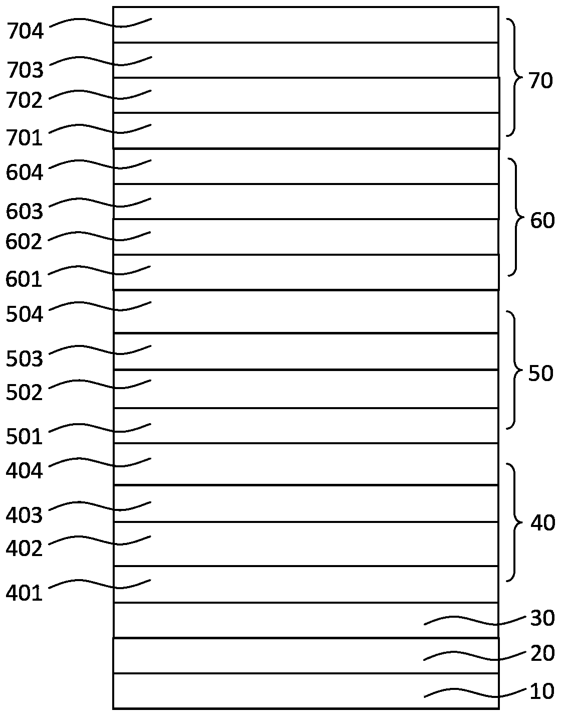
[0139] (4) Prepare the encapsulation layer on the outside of the cathode:

[0140] The encapsulation layer includes 6 overlapping encapsulation layer units, and the encapsulation layer unit includes a first organic barrier layer, a first inorganic barrier layer, a second organic barrier layer, and a second inorganic barrier layer stacked in sequence;

[0141] Production of the first organic barrier layer: the mixture formed by mixing NPB and BCP according to the material ratio of 1:1 is used as the material of the first organic barrier layer, and the vacuum degree is 5×10 -5 Pa, evaporation rate Thickness 250nm;

[0142] Fabrication of the first inorganic barrier layer: AlN, Bi 2 Te 3 The mixture formed by mixing with Al is used as the material of the first inorganic barrier layer, wherein AlN accounts for 10% of the total mass of th...

Embodiment 3

[0147] An organic electroluminescent device is prepared through the following steps:

[0148] (1), (2), (3) are the same as embodiment 1;

[0149] (4) Prepare the encapsulation layer on the outside of the cathode:

[0150] The encapsulation layer includes 6 overlapping encapsulation layer units, and the encapsulation layer unit includes a first organic barrier layer, a first inorganic barrier layer, a second organic barrier layer, and a second inorganic barrier layer stacked in sequence;

[0151] Production of the first organic barrier layer: the mixture formed by mixing TAPC and TPBi according to the material ratio of 1:1 is used as the material of the first organic barrier layer, and the vacuum degree is 5×10 -5 Pa, evaporation rate Thickness 200nm;

[0152] The making of the first inorganic barrier layer: the mixture formed by mixing BN, CdTe and Ni is used as the material of the first inorganic barrier layer, wherein, BN accounts for 30% of the total mass of the first ...


PUM


Abstract

The invention is to provide an organic light-emitting diode with a packaging layer structure. The packaging layer is a composite structure formed by stacking packaging layer units. Each packaging layer unit comprises a first organic barrier layer, a first inorganic barrier layer, a second organic barrier layer and a second inorganic barrier layer which are stacked in sequence, so that erosion of external active materials, such as water and oxygen and the like, on the organic light-emitting diode can be reduced effectively, and the service life of the organic light-emitting diode can be prolonged. The invention also provides a preparation method of the organic light-emitting diode. The preparation method is simple in process, low in raw material and easy for mass preparation.

Description

technical field [0001] The invention relates to the field of organic electroluminescence, in particular to an organic electroluminescence device and a preparation method thereof. Background technique [0002] An organic electroluminescent device (OLED) is an energy conversion device that uses organic materials as light-emitting materials and can convert applied electrical energy into light energy. It has outstanding performances such as ultra-thin, self-luminous, fast response, low power consumption, etc., and has extremely broad application prospects in display, lighting and other fields. [0003] The structure of the organic electroluminescent device is a sandwich structure, and an organic light-emitting layer is sandwiched between the cathode and the anode. The organic substances in the light-emitting layer of OLEDs are very sensitive to pollutants, oxygen and moisture in the atmosphere. Long-term exposure will reduce the light-emitting performance of organic electrolumi...

Claims


Application Information

Patent Timeline
Patent Type & Authority Applications(China)
IPC IPC(8): H01L51/52H01L51/54H01L51/56
CPCH10K50/8445H10K71/00
Inventor 周明杰钟铁涛张娟娟王平
Owner OCEANS KING LIGHTING SCI&TECH CO LTD
Why Eureka
Try Eureka