
Silicon through hole patch board wafer testing system and method

A technology of wafer testing and through-silicon vias, which is applied in the field of electronics, can solve problems such as inflexible testing, high testing costs, fragility and fragility, and achieve low-cost testing solutions and improve testing efficiency.

Inactive Publication Date: 2014-12-03
NAT CENT FOR ADVANCED PACKAGING
View PDF0 Cites 5 Cited by
  • Summary
  • Abstract
  • Description
  • Claims
  • Application Information

AI Technical Summary

Problems solved by technology

[0003] However, because TSV technology is not fully mature in China, the device yield rate is not ideal. Therefore, it is necessary to test the TSV interposer wafer. The traditional flying probe test machine has high density of test components, many layers, and high wiring density. , The circuit board with a small measuring point distance has the advantages of fine pitch, not limited by the grid, flexible testing and fast speed. However, because the thinned TSV adapter wafer is only a few hundred microns thick, it is very fragile Fragile, cannot be fixed directly on the current flying probe tester
At the same time, the sample to be tested on the flying probe testing machine is determined based on the copper frame on the rectangular substrate as the approximate reference position, which cannot be aligned with the reference position of the circular TSV adapter board wafer to be tested. Among them, in order to test the TSV interposer wafer, it is necessary to purchase an automated test system (Automatic Test Equipment, referred to as ATE), an automatic probe station, and for different TSV layouts, it is necessary to customize different probe cards. The test is not flexible and the test high cost

Method used


Image

  • Silicon through hole patch board wafer testing system and method
  • Silicon through hole patch board wafer testing system and method
  • Silicon through hole patch board wafer testing system and method

Examples


Embodiment Construction

[0031] The present invention will be further described in detail below in conjunction with the accompanying drawings and embodiments. It should be understood that the specific embodiments described here are only used to explain the present invention, but not to limit the present invention. In addition, it should be noted that, for the convenience of description, only parts related to the present invention are shown in the drawings but not all content.

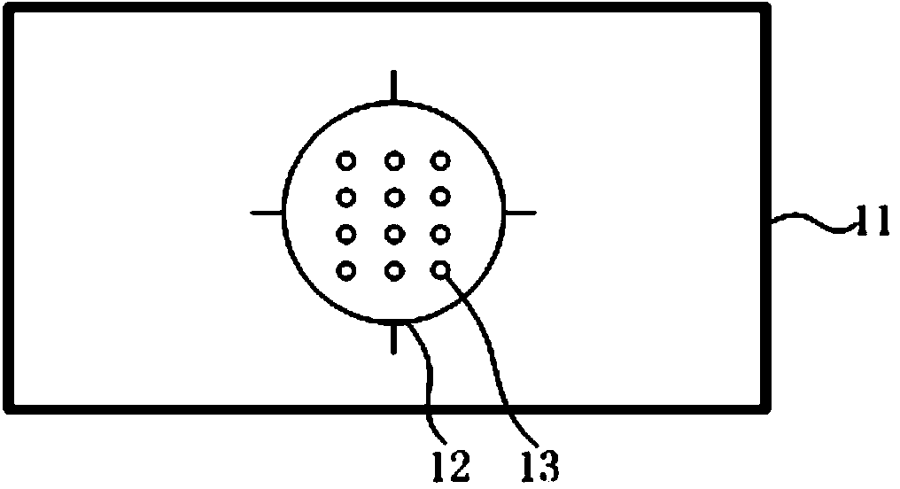
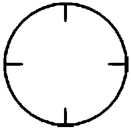
[0032] figure 1 It is a schematic diagram of a circuit board in a TSV interposer wafer testing system provided by an embodiment of the present invention, figure 2 It is a schematic diagram of a TSV interposer wafer to be tested in a TSV interposer wafer testing system provided by an embodiment of the present invention, combined below figure 1 and figure 2 Embodiments of the present invention will be described.

[0033] The TSV adapter wafer testing system includes a flying probe tester and a circuit board, the flying prob...


PUM


Abstract

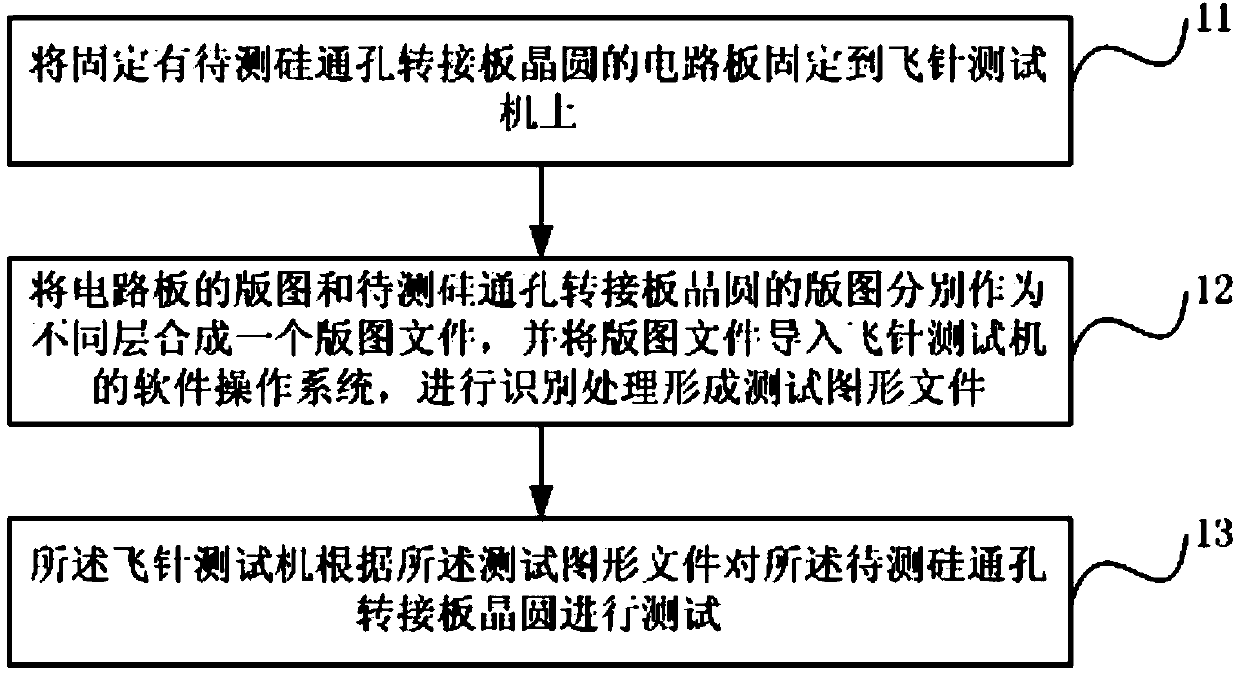
The invention discloses a silicon through hole patch board wafer testing system and method. The system comprises a fly-probe tester and a circuit board, wherein the fly-probe tester is used for testing a silicon through hole patch board wafer to be tested, the circuit board is used for fixing the silicon through hole patch board wafer to be tested to the fly-probe tester, and position alignment marks for alignment with a rack plate frame of the fly-probe tester are provided. According to the silicon through hole patch board wafer testing system and method, the silicon through hole patch board wafer can be automatically tested through the fly-probe tester, silicon through hole patch board wafers with different layouts can be tested, an automatic testing machine and an automatic probe table do not need to be purchased, corresponding expensive probe cards do not need to be customized according to the silicon through hole patch board wafers with different layouts, testing efficiency is improved, and a testing scheme with low cost is provided.

Description

technical field [0001] The invention relates to the field of electronic technology, in particular to a wafer testing system for a through-silicon via adapter board and a wafer testing method for a through-silicon via adapter board. Background technique [0002] With the rapid development of electronic products, microelectronic packaging technology is developing towards the trend of multi-function, miniaturization, portability, high speed, low power consumption and high reliability. System In a Package (SIP for short) can effectively reduce the chip area, and Through Silicon Via (TSV for short) technology is an important technology in the SIP packaging process. Layer chips are interconnected, so TSV has received more and more attention. [0003] However, because TSV technology is not fully mature in China, the device yield rate is not ideal. Therefore, it is necessary to test the TSV interposer wafer. The traditional flying probe test machine has high density of test compone...

Claims


Application Information

Patent Timeline
IPC IPC(8): G01R31/26G01R1/067
Inventor 杜天敏
Owner NAT CENT FOR ADVANCED PACKAGING
Learn More