High-energy ion injection device

An ion implantation device and high-energy technology, which is applied in the manufacture of discharge tubes, electrical components, semiconductors/solid-state devices, etc., to achieve the effect of ensuring energy accuracy and suppressing divergence

Active Publication Date: 2014-12-03
SENCORP
View PDF12 Cites 5 Cited by
  • Summary
  • Abstract
  • Description
  • Claims
  • Application Information

AI Technical Summary

Problems solved by technology

[0013] However, in the production of high-quality imaging elements, not only angular accuracy is required, but also many strict requirements such as no metal contamination, small implant d

Method used


Image

  • High-energy ion injection device
  • High-energy ion injection device
  • High-energy ion injection device

Examples


Embodiment Construction

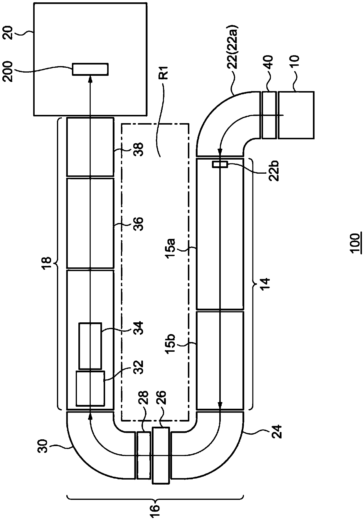
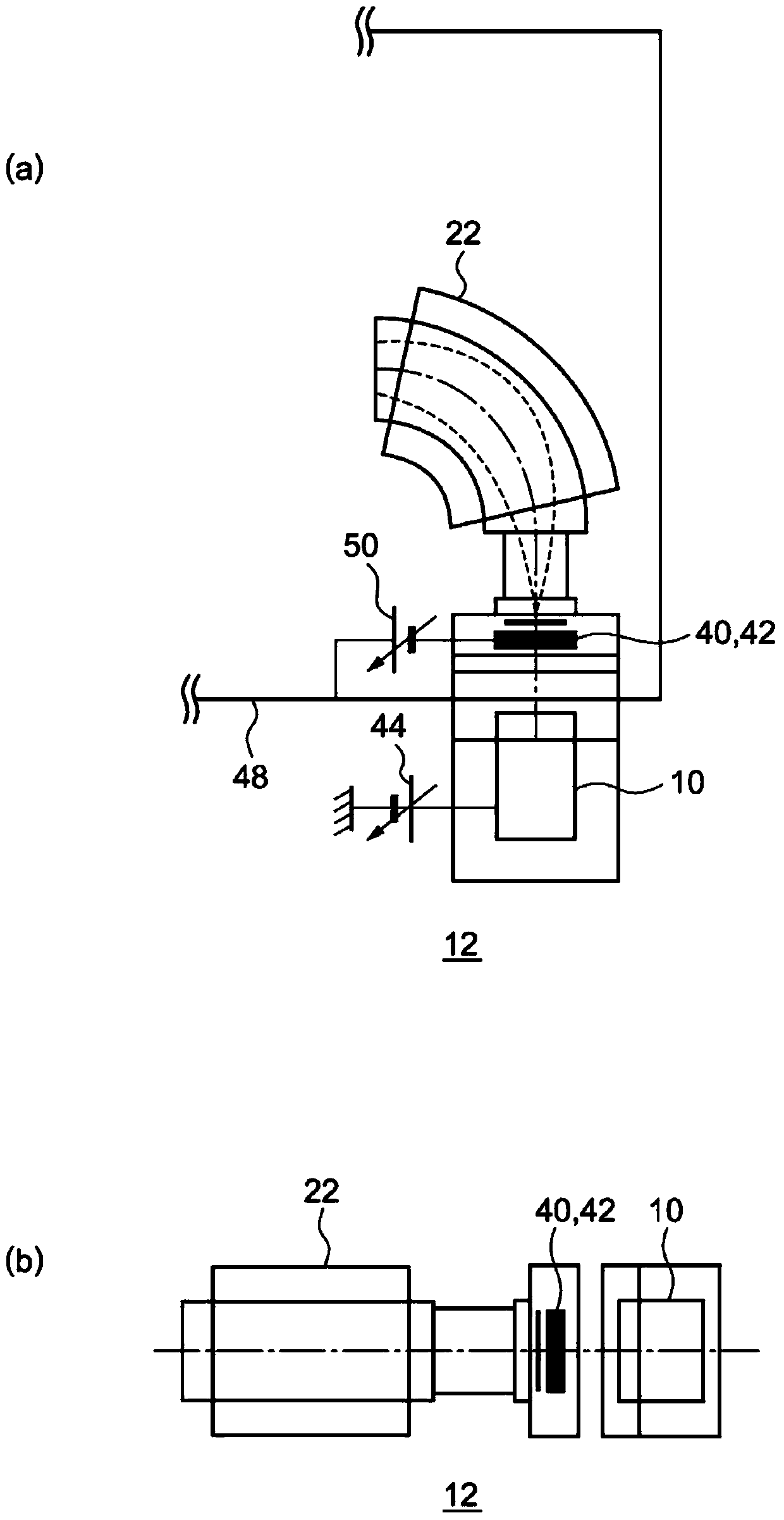
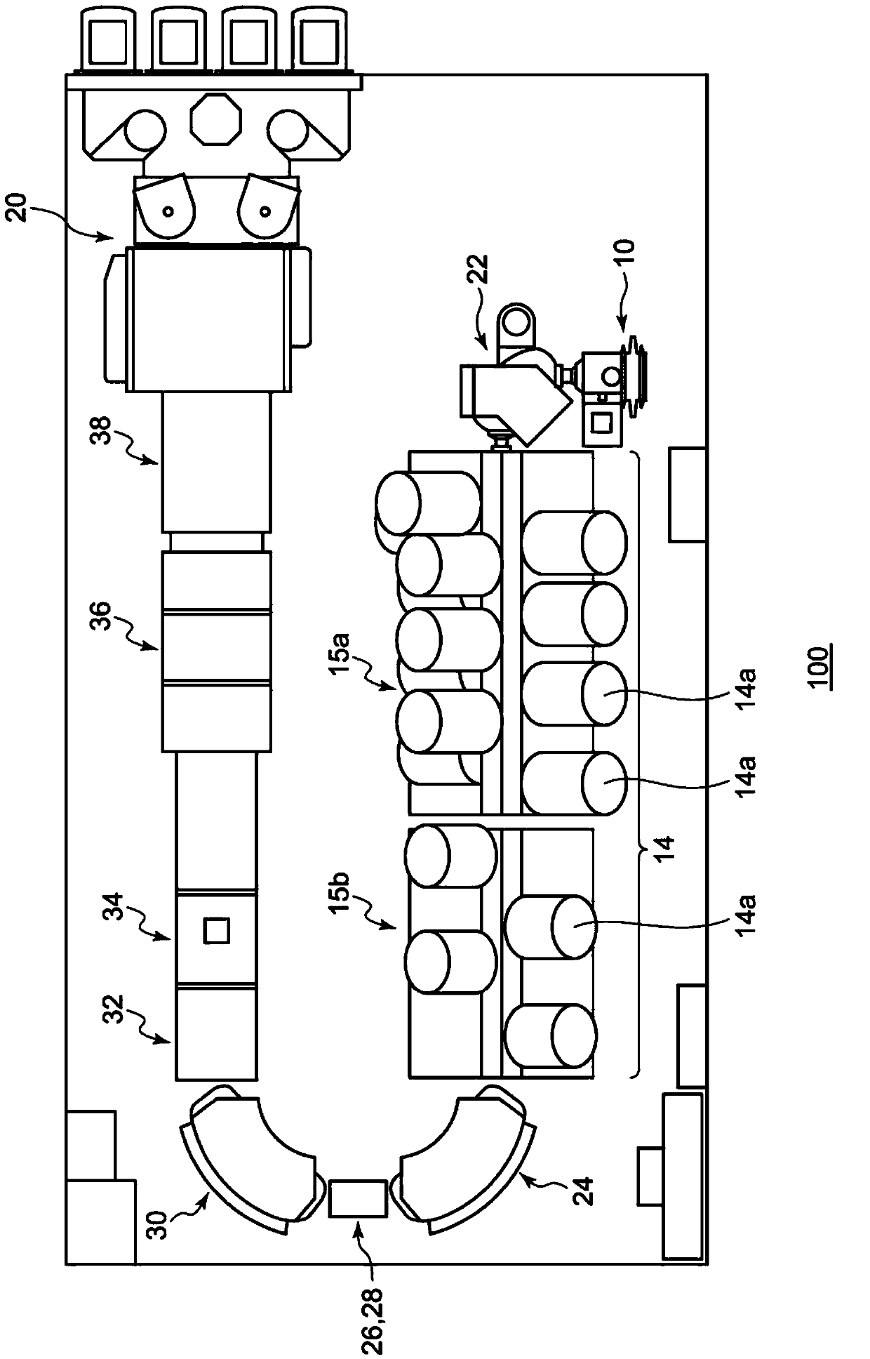
[0044] An example of the high-energy ion implantation apparatus according to this embodiment will be described in more detail below. First, the process by which the present inventors conceived the present invention will be described.

[0045] (parallel magnet)

[0046] A conventional high-energy ion implanter using a parallelizing magnet for parallelizing tracks by a deflection magnetic field has the following problems.

[0047] If high-energy ions are implanted into a wafer with a photoresist layer, a large amount of air leakage will occur, and the molecules of the air leakage will interact with beam ions, and the valence numbers of some ions will change. When the valence changes when passing through the parallelizing magnet, the deflection angle changes, so the parallelism of the beam is broken, and the injection angle toward the wafer becomes different.

[0048] In addition, the amount (number or dose) of implanted ions is obtained by measuring the beam current value with...


PUM


Abstract

The present invention provides a high-energy ion injection device, which carries out scanning, parallelization, and filtering on high-energy ion beams through an electric field. The high-energy ion injection device (100) comprises: a high energy multi-segment straight line accelerating unit (14), which accelerates the ion beam and thereby generating the high-energy ion beam; a deflection unit (16), which carries out direction conversion on the high-energy ion beam toward a semiconductor wafer; irradiation beam transmission line unit (18), which transmits the deflected high-energy ion beam to the wafer. The irradiation beam transmission line unit (18) comprises an irradiation beam reshaper (32), a high-energy irradiation beam scanner (34), and a high-energy electric field irradiation beam parallelization device (36), and an electric field final energy filter (38).

Description

technical field [0001] This application claims priority based on Japanese Patent Application No. 2013-113474 filed on May 29, 2013. The entire content of this application is incorporated in this specification by reference. [0002] The invention relates to a high-energy ion implantation device. Background technique [0003] In the manufacturing process of semiconductor elements, an important process for adding impurities to the crystal of the semiconductor wafer by implanting ions into the semiconductor wafer under vacuum to change the conductivity and make the semiconductor Wafer semiconductor components. The device used in this process is called an ion implantation device, and the ion implantation device accelerates impurity atoms as ions and implants them into the semiconductor wafer. [0004] With the high integration and high performance of semiconductor elements, devices capable of performing high-energy ion implantation to penetrate deeper into semiconductor wafers...

Claims


Application Information

Patent Timeline
IPC IPC(8): H01J37/317
CPCH01J37/05H01J37/3171H01J2237/04737H01J2237/053H01J2237/057H01L21/26506
Inventor 椛泽光昭渡边一浩佐佐木玄稻田耕二
Owner SENCORP
Why Eureka
Try Eureka