Organic light emitting device and manufacturing method thereof

An electroluminescence device and luminescence technology, which is applied in the manufacture of organic semiconductor devices, electric solid state devices, semiconductor/solid state devices, etc., can solve the problems of small driving current, low device life, and large current for driving light emitting devices

Inactive Publication Date: 2014-12-03
OCEANS KING LIGHTING SCI&TECH CO LTD +2
View PDF4 Cites 18 Cited by
  • Summary
  • Abstract
  • Description
  • Claims
  • Application Information

AI Technical Summary

Problems solved by technology

[0003] So far, although researchers from all over the world have greatly improved the performance indicators of the device by selecting suitable organic materials and reasonable device structure design, due to the large current driving the light-emitting device

Method used


Image

  • Organic light emitting device and manufacturing method thereof
  • Organic light emitting device and manufacturing method thereof

Examples


Embodiment 1

[0048] A method for preparing an organic electroluminescent device, comprising the following steps:

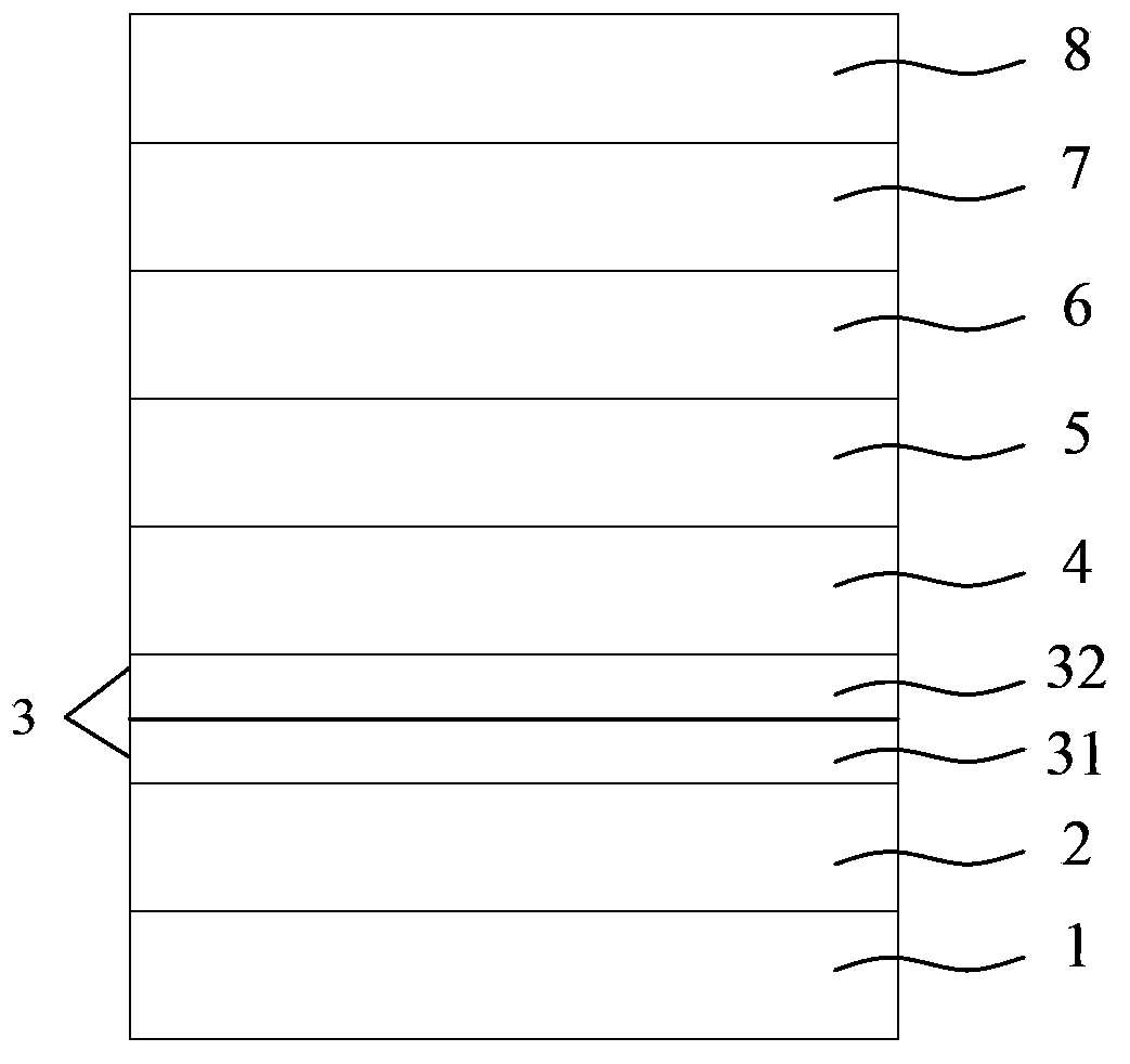
[0049] (1) After rinsing the glass substrate with distilled water and ethanol, soak it in isopropanol overnight. On the glass substrate 1, the anode 2 is prepared by magnetron sputtering to obtain the anode substrate. The material of the anode 2 is ITO, the thickness is 70nm, the sputtering rate is 0.2nm / s, and the pressure during magnetron sputtering is 1×10 -5 ;

[0050] (2) Put the anode substrate into the vapor deposition chamber, feed hydrogen to maintain the pressure of the vapor deposition chamber at 10Pa, then raise the temperature of the vapor deposition chamber to 600°C, and then feed methane to maintain the pressure of the vapor deposition chamber at 10Pa , on the anode substrate, a graphene film is prepared by vapor deposition, and after the reaction is completed, a graphene film with a thickness of 4nm is obtained;

[0051] Transfer the graphene film into the pl...

Embodiment 2

[0063] A method for preparing an organic electroluminescent device, comprising the following steps:

[0064] (1) After rinsing the glass substrate with distilled water and ethanol, soak it in isopropanol for one night. The anode was prepared by magnetron sputtering on the glass substrate, and the anode substrate was obtained. The material of the anode was IZO, the thickness was 200nm, the sputtering rate was 2nm / s, and the pressure during magnetron sputtering was 1×10 -3 ;

[0065] (2) Put the anode substrate into the vapor deposition chamber, feed hydrogen to maintain the pressure of the vapor deposition chamber at 1000Pa, then raise the temperature of the vapor deposition chamber to 1000°C, and then feed ethane to maintain the pressure of the vapor deposition chamber at 1000Pa, prepare a graphene film by vapor deposition on the anode substrate; after the reaction is completed, a graphene film with a thickness of 10nm is obtained;

[0066] Graphene thin film is transferred ...

Embodiment 3

[0078] A method for preparing an organic electroluminescent device, comprising the following steps:

[0079] (1) After rinsing the glass substrate with distilled water and ethanol, soak it in isopropanol overnight. The anode was prepared by magnetron sputtering on the glass substrate, and the anode substrate was obtained. The anode material was AZO, the thickness was 80nm, the sputtering rate was 1nm / s, and the pressure during magnetron sputtering was 1×10 -4 ;

[0080] (2) Put the anode glass substrate into the vapor deposition chamber, feed hydrogen to maintain the pressure of the vapor deposition chamber at 500 Pa, then raise the temperature of the vapor deposition chamber to 800°C, and then feed propane to maintain the pressure of the vapor deposition chamber at 600Pa, a graphene film is prepared by chemical vapor deposition on the anode substrate; after the reaction is completed, a graphene film with a thickness of 8nm is obtained;

[0081] The graphene film is transfer...


PUM

PropertyMeasurementUnit
Thicknessaaaaaaaaaa
Thicknessaaaaaaaaaa
Thicknessaaaaaaaaaa

Abstract

The invention discloses an organic light emitting device, which comprises a glass substrate, an anode, a hole injection layer, a hole transmission layer, a light emitting layer, an electron transmission layer, an electron injection layer, and a cathode stacked in sequence, wherein the hole injection layer comprises a graphene oxide layer and a metallic oxide layer. The hole injection layer has a two-layer structure, the original hole injection barrier is separated into two parts, the hole firstly jumps into the graphene oxide layer from the anode and then jumps into the metallic oxide layer form the graphene oxide layer, and the hole is finally injected into the hole transmission material from the metallic oxide layer, and therefore, starting voltage of the device is reduced, and the light efficiency is improved. The invention also discloses an organic light emitting device manufacturing method. Graphene is adopted as raw material, the graphene oxidation process can be realized in a simple oxidation method, and the preparation method is simple.

Description

technical field [0001] The invention relates to the field of organic electroluminescence, in particular to an organic electroluminescence device and a preparation method thereof. Background technique [0002] Organic Light Emission Diode (hereinafter referred to as OLED) has the characteristics of high brightness, wide range of material selection, low driving voltage, fully cured active luminescence, etc., and has the advantages of high definition, wide viewing angle, and fast response speed. It is a display technology and light source with great potential, which conforms to the development trend of mobile communication and information display in the information age, as well as the requirements of green lighting technology, and is the focus of many researchers at home and abroad. [0003] So far, although researchers from all over the world have greatly improved the performance indicators of the device by selecting suitable organic materials and reasonable device structure d...

Claims


Application Information

Patent Timeline
IPC IPC(8): H01L51/52H01L51/54H01L51/56
CPCH10K50/17H10K2102/00H10K71/00
Inventor 周明杰冯小明陈吉星王平
Owner OCEANS KING LIGHTING SCI&TECH CO LTD
Why Eureka
Try Eureka