Supercharge Your Innovation With Domain-Expert AI Agents!

AMOLED (Active Matrix Organic Light Emitting Diode) structure and production method thereof

A manufacturing method and packaging layer technology, applied in semiconductor/solid-state device manufacturing, electrical components, electric solid-state devices, etc., can solve problems such as thinning and inability to fully utilize the back of TFT, and achieve the effect of reducing the overall thickness

Active Publication Date: 2014-12-10
EVERDISPLAY OPTRONICS (SHANGHAI) CO LTD
View PDF5 Cites 0 Cited by
  • Summary
  • Abstract
  • Description
  • Claims
  • Application Information

AI Technical Summary

Problems solved by technology

[0005] The purpose of the present invention is to overcome the defects of the prior art, to provide an AMOLED structure and its manufacturing method, which can solve the problem that the back of the TFT in the AMOLED cannot be fully utilized, so as to achieve the effect of thinning the thickness of the AMOLED

Method used


Image

  • AMOLED (Active Matrix Organic Light Emitting Diode) structure and production method thereof
  • AMOLED (Active Matrix Organic Light Emitting Diode) structure and production method thereof
  • AMOLED (Active Matrix Organic Light Emitting Diode) structure and production method thereof

Examples


Embodiment Construction

[0032] The present invention will be further described below in conjunction with the accompanying drawings and specific embodiments.

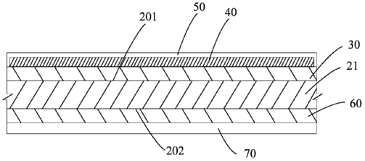
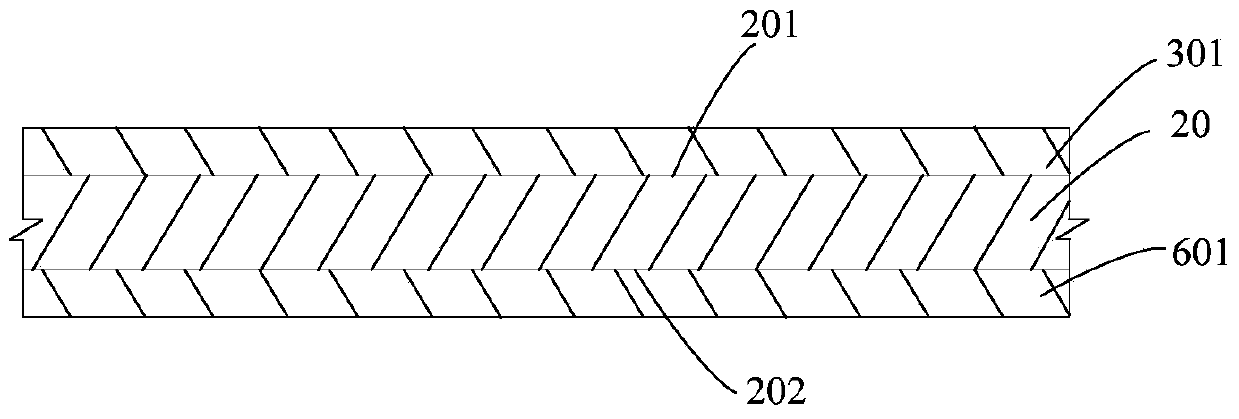
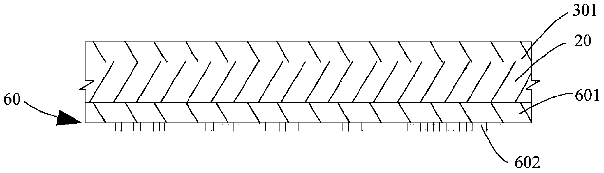
[0033] see figure 1 , shows a schematic cross-sectional view of an AMOLED structure of the present invention. The AMOLED structure of the present invention discloses a kind of AMOLED structure in which a semiconductor silicon chip is used to replace plexiglass as a substrate, and the back side of the substrate is used to make a mainboard circuit. The original substrate of the motherboard circuit and the wiring space for electrical connection between the motherboard circuit and the TFT circuit can effectively reduce the overall thickness of the AMOLED. In the packaging of the existing AMOLED structure, the TFT circuit and the OLED device layer are formed on the glass substrate, and then the main board circuit is made separately, and the main board circuit and the TFT circuit are electrically connected, and then the above structures are packaged ...


PUM


Abstract

The invention relates to an AMOLED (Active Matrix Organic Light Emitting Diode) structure and a production method thereof. The AMOLED structure comprises a substrate, a TFT (Thin Film Transistor) circuit layer, a mainboard circuit layer, an OLED (Organic Light Emitting Diode) device layer, a first encapsulation layer and a second encapsulation layer; the substrate comprises a top surface and a bottom surface which are opposite to each other; the TFT circuit layer is arranged on the top surface of the substrate; the mainboard circuit layer is arranged on the bottom surface of the substrate; the OLED device layer is arranged above the TFT circuit layer; the first encapsulation layer wraps the TFT circuit layer and the OLED device layer; the second encapsulation layer wraps the mainboard circuit layer. According to the AMOLED structure and the production method thereof, the space of the substrate can be effectively utilized and meanwhile the thickness of the AMOLED can be reduced.

Description

technical field [0001] The invention relates to the display field, in particular to an AMOLED structure and a manufacturing method thereof. Background technique [0002] Organic light emitting diode (Organic Light) Emitting Diode, OLED) has the characteristics of self-illumination, using a very thin organic material coating and glass substrate, when the current passes through, the organic material will emit light, and the organic light emitting diode display screen viewing angle Large, and can significantly save power, so the application of organic light-emitting diodes is becoming more and more extensive. The drive mode of OLED is divided into passive drive and active drive, passive drive is passive drive (PMOLED, Passive Matrix Organic Light Emitting Diode (passive organic electroluminescent diode), active drive is active drive (AMOLED, Active Matrix Organic Light Emitting Diode (Active Matrix Organic Light Emitting Diode panel). Due to the difficulty of large-scale PMOLE...

Claims


Application Information

Patent Timeline
IPC IPC(8): H01L27/32H01L51/56
Inventor 邓学易
Owner EVERDISPLAY OPTRONICS (SHANGHAI) CO LTD
Features
  • R&D
  • Intellectual Property
  • Life Sciences
  • Materials
  • Tech Scout
  • Unparalleled Data Quality
  • Higher Quality Content
  • 60% Fewer Hallucinations
Learn More