Touch-panel-equipped liquid crystal display device
A liquid crystal display device, touch panel technology, applied in the input/output process of data processing, instruments, polarizing elements, etc., can solve problems such as cracks in electrode patterns, and achieve the effect of preventing cracks
- Summary
- Abstract
- Description
- Claims
- Application Information
AI Technical Summary
Problems solved by technology
Method used
Image
Examples
Embodiment 1
[0388]
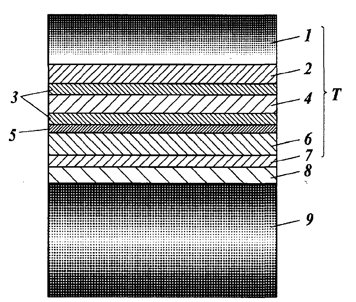
[0389] An ITO film was formed on tempered glass with a thickness of 20 nm by a sputtering method, and a first electrode pattern in the X direction was formed by etching.
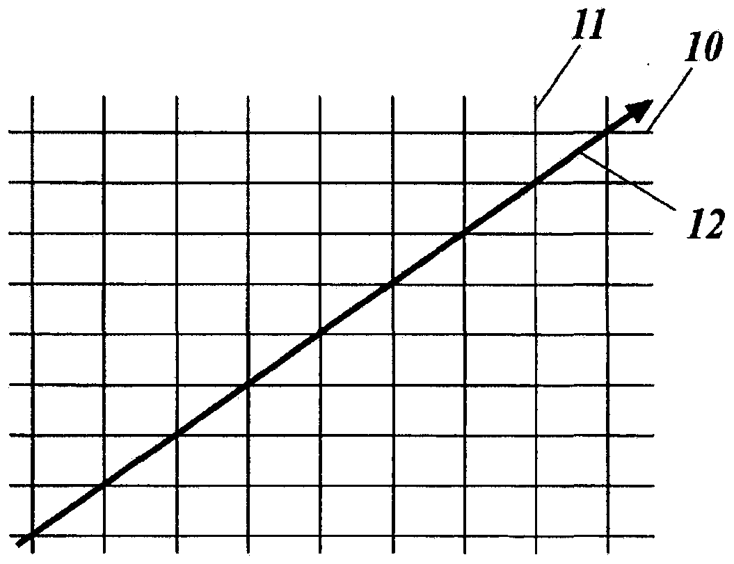
[0390] Next, as an insulating layer arranged between the electrode patterns, SiO2 is formed into a film with a thickness of 200 nm by sputtering, and an ITO film is formed on top of it with a thickness of 20 nm by sputtering, and a grid pattern is formed by etching. A second electrode pattern in the Y direction is formed. Then, as an insulating layer, SiO was sputtered 2 Film formation was performed with a thickness of 200 nm.
[0391] It was connected to a control circuit via lead wires prepared by coating and firing Ag paste on the formed ITO electrode patterns in the X direction and Y direction, respectively.
[0392] Next, the glass-scattering prevention film (cellulose ester film A1) produced under the following conditions was cut out, and it bonded on the 2nd electrode pattern via the adhe...
Embodiment 2
[0477]
[0478] On the respective surfaces of the cellulose ester films A1 to A5, COP films, PC films, and PET films prepared above, the following hard coat composition 1 was coated with a 0.4 μm pore size film using an extrusion coater. The solution filtered through a polypropylene filter was dried at a temperature of 80°C, and then cleaned with nitrogen so that the oxygen concentration was 1.0% by volume or less, and the illuminance of the irradiated part was 100mW / cm using an ultraviolet lamp. 2 , so that the irradiation dose is 0.25J / cm 2 Then, the coating layer was cured to form a hard coat layer 1 having a dry film thickness of 3 μm, and was wound up to produce roll-shaped hard coat films A1H to A5H, COP film H, PC film H, and PET film H.
[0479]
[0480] The following materials were stirred and mixed to form a hard coat coating composition 1 .
[0481] pentaerythritol tri / tetraacrylate
[0482] (NK Ester A-TMM-3L, manufactured by Shin-Nakamura Chemical Industry C...
Embodiment 3
[0493] Using the liquid crystal display devices 1 to 13 with a touch panel prepared in Example 1, the liquid crystal display parts were observed without wearing polarized sunglasses. As a result, there was no problem at all levels, especially in terms of visibility.
[0494] Wearing polarized sunglasses to observe the liquid crystal display part, as a result, the liquid crystal display devices 11-13 with touch panels of the comparative examples have poor visibility, and the liquid crystal display devices 1, 2, 6-10 with touch panels of the present invention Since the retardation value of the anti-glass scattering film is within a preferable range, and it is bonded to a liquid crystal display panel at a preferable angle, there is no defect in the image and the visibility is good. In the liquid crystal display devices 3 to 5 with a touch panel according to the present invention, the retardation value of the glass scatter prevention film was insufficient, which may be the result o...
PUM
| Property | Measurement | Unit |
|---|---|---|
| Thickness | aaaaa | aaaaa |
| Thickness | aaaaa | aaaaa |
| Roll length | aaaaa | aaaaa |
Abstract
Description
Claims
Application Information


