Acceleration sensor chip capable of resisting transverse effect and manufacturing method thereof

An acceleration sensor and lateral effect technology, applied in the direction of acceleration measurement using inertial force, can solve the problems of large lateral sensitivity, large device volume, and low natural frequency

Inactive Publication Date: 2014-12-24
XI AN JIAOTONG UNIV
View PDF5 Cites 11 Cited by
  • Summary
  • Abstract
  • Description
  • Claims
  • Application Information

AI Technical Summary

Problems solved by technology

While these proposals are effective, these additional operations lead to high costs, low reliability, and errors in processing
[0003] The traditional piezoresistive micro-acceleration sensor is generally a cantilever beam structure or a double-ended fixed-supported beam structure. The cantilever beam structure has high sensitivity, but its natural frequency is low and its lateral sensitivity is large; the double-ended fixed-supported beam structure has high natural frequency and low lateral sensitivity. The sensitivity is low, and the processed device is large in size and low in cost performance

Method used


Image

  • Acceleration sensor chip capable of resisting transverse effect and manufacturing method thereof
  • Acceleration sensor chip capable of resisting transverse effect and manufacturing method thereof
  • Acceleration sensor chip capable of resisting transverse effect and manufacturing method thereof

Examples


Embodiment Construction

[0030] The present invention will be described in more detail below in conjunction with the accompanying drawings.

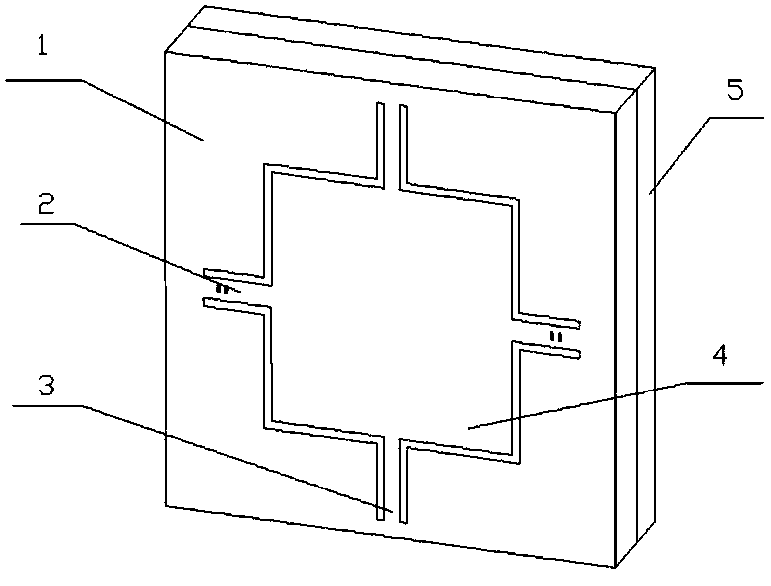
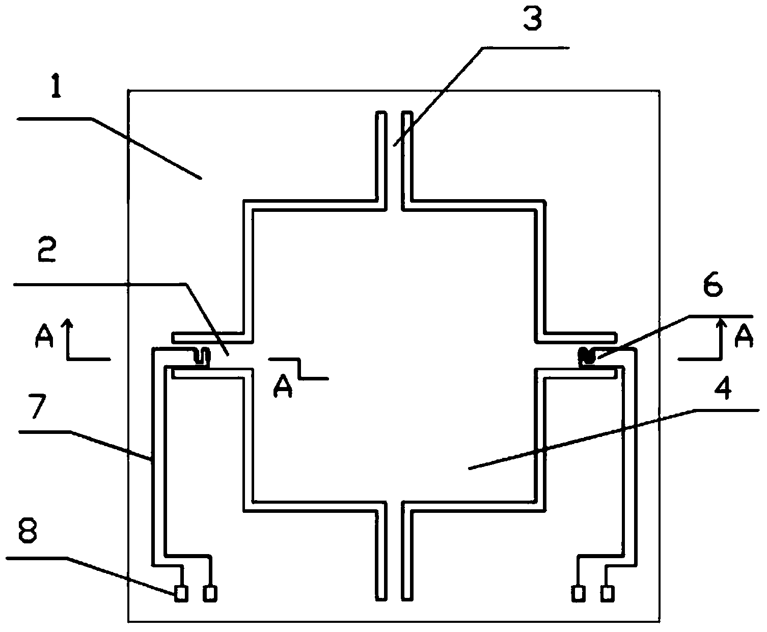
[0031] refer to figure 1 , an acceleration sensor chip with low lateral effect, comprising a silicon substrate 1, the back of the silicon substrate 1 is bonded to boron glass 5, a suspended mass 4 is arranged in the central cavity of the silicon substrate 1, and two identical complementary The beams 3 are respectively connected with one set of opposite sides of the suspended mass 4, and the two same sensitive beams 2 are respectively connected with the other set of opposite sides of the suspended mass, and the supplementary beam 3 and the sensitive beam 2 jointly support the suspended mass 4, so that It remains in a suspended state, and a working gap is reserved between the boron glass 5 and the bottom surface of the suspended mass 4 to ensure that the suspended mass 4 can always be suspended in the air when the sensor is working normally. contact, to prevent o...


PUM


Abstract

The invention relates to an acceleration sensor chip capable of resisting the transverse effect and a manufacturing method of the acceleration sensor chip. According to the chip, a pair of sensitive beams and a pair of supplementary beams jointly support a suspended mass block of the chip and make the suspended mass block be suspended. Piezoresistors are arranged on the sensitive beams and connected to form a semi-open-loop Wheatstone bridge. The output end of the Wheatstone bridge is connected with a pad of the chip. The manufacturing method comprises the steps that through anisotropic wet etching of silicon and ICP etching, a movable structure located in a silicon substrate is obtained, wherein the movable structure is composed of the suspended mass block, the sensitive beams and the supplementary beams; positive photo-etching and sputtering are performed to form a metal lead and the pad of the chip; borax glass is pasted on the reverse of the silicon substrate; positive photo-etching and etching are performed to form a gap between the movable component of the chip and the silicon substrate; finally, the chip is obtained. The chip can meet the performance requirements for high sensitivity, low range and low resonant frequency and meanwhile has the good feature for resisting the transverse effect.

Description

technical field [0001] The invention relates to the technical field of micro-acceleration sensor chips, in particular to an acceleration sensor chip with low lateral effect and a manufacturing method thereof. Background technique [0002] The early silicon micro-accelerometer was invented in 1979. Since then, MEMS acceleration sensors have achieved great success in many commercial fields under the stimulation of the advantages of body processing and surface processing micromechanical technology, namely low energy consumption, miniaturization, and low cost. . The variety of transduction mechanisms allows MEMS accelerometers to replace conventional sensors in many applications. Among these sensors, piezoresistive accelerometers play an important role in monitoring vibrations, and such sensors have achieved success in many different sensor configurations, such as cantilever-mass structures, counter structures, and dual-mass structures. In addition, there are two recent resear...

Claims


Application Information

Patent Timeline
Patent Type & Authority Applications(China)
IPC IPC(8): G01P15/12
Inventor 田边韩佰锋赵玉龙蒋庄德马婧曌
Owner XI AN JIAOTONG UNIV
Why Eureka
Try Eureka