Method for efficiently fabricating high-precision multi-step microlens arrays
A microlens array and multi-step technology, which is applied in the direction of lens, microlithography exposure equipment, and photolithography exposure equipment, etc., can solve the problems of high cost and long production time, so as to save production cost, improve production efficiency, and save cost effect
- Summary
- Abstract
- Description
- Claims
- Application Information
AI Technical Summary
Problems solved by technology
Method used
Image
Examples
Embodiment 1
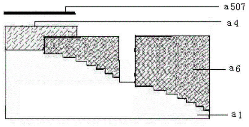
[0039] The present invention provides a method for ingeniously manufacturing a multi-step microlens array, which is applied to a sixteen-step silicon microlens array. The specific implementation scheme includes:
[0040] 1.1.1, one etching, see figure 1 .
[0041] 1) Clean the silicon substrate a1, spin-coat a layer of sacrificial layer a2, then grow a chromium film a3, and finally spin-coat a layer of positive photoresist a4;
[0042] 2) Photolithographic development is carried out with the mask plate a501, where the mask plate a501 includes eight annular zones, and the photoresist exposure and development area is equal to the dry etching area;
[0043] 3) removing the chromium film a3 on the surface of the silicon substrate a1, and cleaning the positive photoresist a4;
[0044] 4) Etching the sacrificial layer a2 to expose the region that needs to be dry-etched, performing one-time etching by dry-etching technology, and taking out the silicon substrate a1 after etching. ...
Embodiment 2
[0078] The present invention provides a method for ingeniously manufacturing a multi-step microlens array, which is applied to a sixteen-step quartz microlens array. The specific implementation scheme includes:
[0079] 2.1.1, one etching, see Figure 11 .
[0080] 1) Clean the quartz substrate b1, grow the chromium film b2, and then spin-coat a layer of positive photoresist b4;
[0081] 2) Photolithographic development is carried out with the mask b501, where the mask b501 includes eight annular zones, and the photoresist exposure and development area is equal to the dry etching area;
[0082] 3) removing the chromium film b2 on the surface of the quartz substrate b1, and cleaning the positive photoresist b3;
[0083] 4) Etching the area to be dry-etched once using dry etching technology, and taking out the quartz substrate b1 after etching.
[0084] 2.1.2, secondary etching, please refer to Figure 12 .
[0085] 1) Clean the quartz substrate b1 first, and spin-coat a la...
Embodiment 3
[0116] The present invention provides a method for ingeniously manufacturing a multi-step microlens array, which is applied to an eleven-step microlens array, and only needs to retain the manufacturing technology of eleven steps and below, and remove the manufacturing technology of more than eleven steps. In a specific embodiment, the mask plate 501a or 501b only includes five rings in the first etching; the mask 502a or 502b only includes two rings in the second etching; the mask 503a in the third etching Or 503b only includes three rings; the mask plate 504a or 504b only includes three rings in four etchings; the mask 505a or 505b only includes one ring in five etchings; The stencil 506a or 506b only includes two rings; the mask 507a or 507b only includes one ring in the seven etchings, and other processes are similar to those in Embodiment 1.
PUM
 Abstract
Description
Claims
Application Information


