Packaging method for board level fan-out structures
A packaging method and fan-out technology, applied in semiconductor devices, electrical components, circuits, etc., can solve the problems of mechanical warpage manufacturing efficiency of board-level fan-out structure, low board-level fan-out structure, etc., to ensure quality and performance, the effect of improving production efficiency
- Summary
- Abstract
- Description
- Claims
- Application Information
AI Technical Summary
Problems solved by technology
Method used
Image

Examples
Embodiment Construction
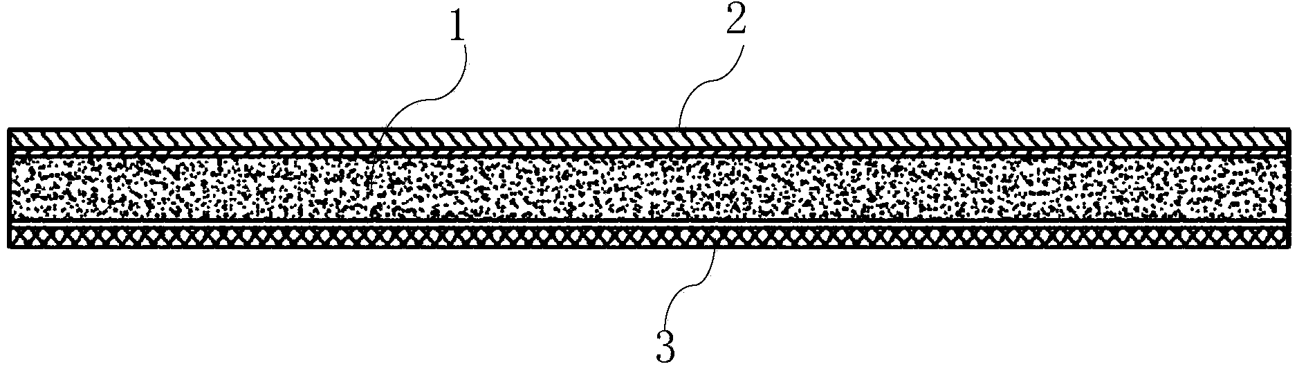
[0029] see figure 1 , an embodiment of the present invention provides a packaging method for a board-level fan-out structure, including:
[0030] Step 1: See figure 1 , press the first double-layer copper foil 2 on the upper side of the core board 1 (using prepreg or double-sided copper-clad organic substrate), and press the second double-layer copper foil 3 on the lower side of the core board 1; The layer copper foil 2 and the second double-layer copper foil 3 are peelable structures. The thickness of the outer layer copper foil in the first double layer copper foil 2 is greater than the thickness of the inner layer copper foil; the thickness of the outer layer copper foil in the second double layer copper foil 3 is greater than the thickness of the inner layer copper foil.
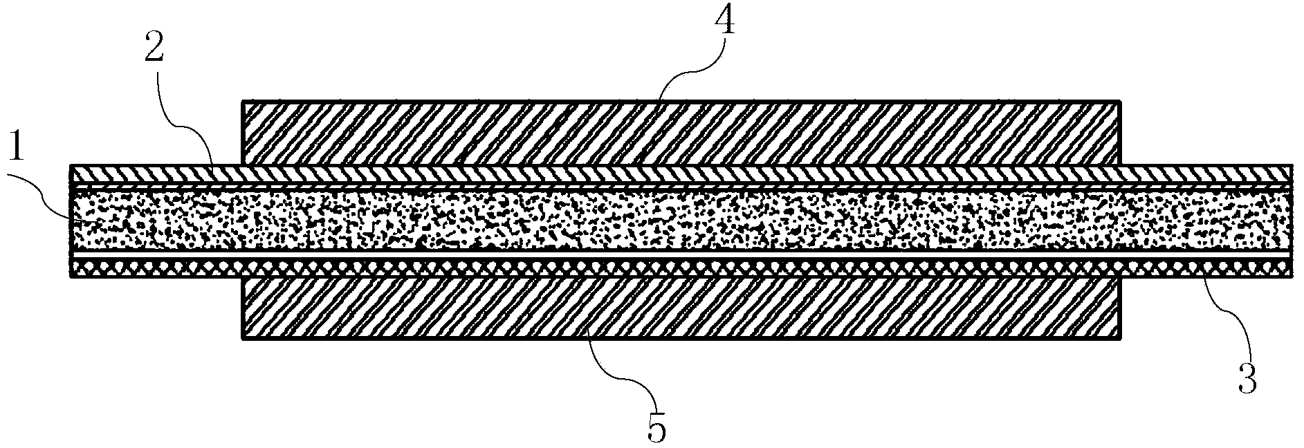
[0031] Step 2: See figure 2 The first chip 4 is mounted on the outside of the first double-layer copper foil 2, the second chip 5 is mounted on the outside of the second double-layer copper foil 3, a...
PUM
 Abstract
Description
Claims
Application Information