A conduction cooling stack semiconductor laser packaging structure

A technology of conduction cooling and packaging structure, used in semiconductor lasers, lasers, laser components and other directions, can solve the problems of poor system integration, large packaging structure and other problems, achieve high power output, improve heat dissipation performance, and achieve the effect of power output

Active Publication Date: 2017-02-15
FOCUSLIGHT TECH
View PDF6 Cites 1 Cited by
  • Summary
  • Abstract
  • Description
  • Claims
  • Application Information

AI Technical Summary

Problems solved by technology

[0008] The present invention proposes a new conduction-cooled stacked semiconductor laser packaging structure, which solves the problems of large volume and poor system integration of the existing packaging structure

Method used


Image

  • A conduction cooling stack semiconductor laser packaging structure
  • A conduction cooling stack semiconductor laser packaging structure
  • A conduction cooling stack semiconductor laser packaging structure

Examples


Embodiment Construction

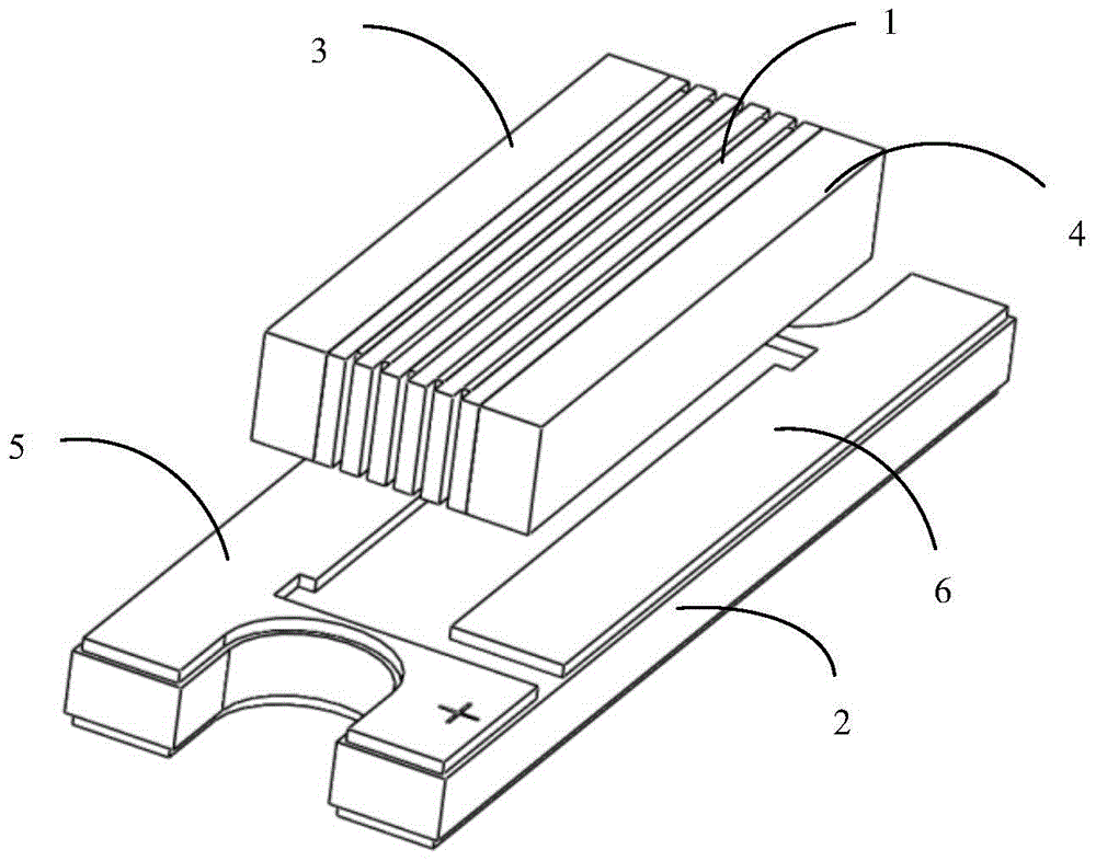
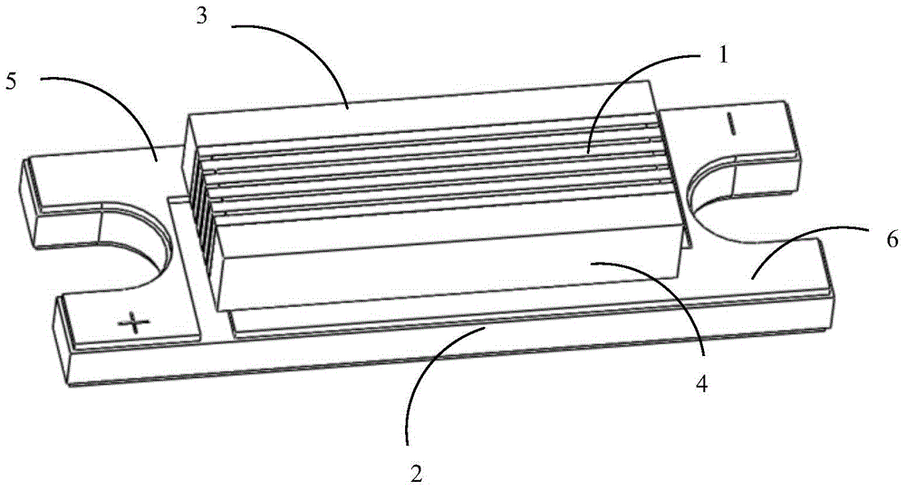
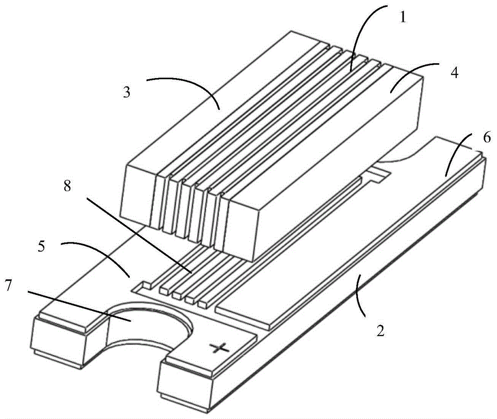
[0036] Such as figure 1 As shown, the conduction cooling stacked semiconductor laser packaging structure of the present invention includes a laser chip group 1 and an insulating heat sink 2, and the laser chip group 1 adopts a plurality of laser chips to form a stacked module, wherein each laser chip has a substrate ; The two end faces of the array module chip stacking direction are bonded and welded with a positive connection block 3 and a negative connection block 4; the surface of the insulating heat sink is provided with two L-shaped conductive sheets that are not in contact with each other in a centrosymmetric manner , respectively as the positive electrode 5 and the negative electrode 6; the bottoms of the positive connection block 3 and the negative connection block 4 are respectively welded and fixed to the long parts of the two L-shaped conductive sheets, and the stacked module 1 corresponds to the two L-shaped The conductive sheet surrounds a rectangular strip area ...


PUM


Abstract

The invention provides a packaging structure of a conduction-cooled stack semiconductor laser and solves the problems that the existing packaging structure is larger in size and system integration is poor. The packaging structure is characterized in that an anode connection block and a cathode connection block are attached and welded to two end faces of a stack module in the chip stacking direction; two L-shaped conductive sheets in no contact with each other are arranged on the surface of an insulating heat sink in a central symmetry manner and serve as an outgoing anode and an outgoing cathode, respectively; the bottom of the anode connection block and the bottom of the cathode connection block are correspondingly welded and fixed to elongated portions of the L-shaped conductive sheets; the stack module surrounds an area on the surface of the insulating heat sink in correspondence to the L-shaped conducive sheets; a short portion of each L-shaped conductive sheet is provided with a mounting hole.

Description

technical field [0001] The invention relates to a conduction cooling stack semiconductor laser packaging structure, which is especially suitable for high-power semiconductor laser pumping solid-state lasers or direct lighting applications. Background technique [0002] Semiconductor lasers have the advantages of small size, light weight, high electro-optical conversion efficiency, high reliability and long life, and can be widely used in pumping solid-state and fiber lasers. These lasers can be used in laser information transmission, material processing, medical treatment and beauty, Scientific research, laser printing, military defense and laser entertainment display; it can also be directly applied to material surface treatment, laser night vision lighting system, laser hair removal and other fields after optical shaping. More and more applications require semiconductor lasers to have higher power density, longer life, higher stability and reliability, and longer storage t...

Claims


Application Information

Patent Timeline
Patent Type & Authority Patents(China)
IPC IPC(8): H01S5/00H01S5/024H01S5/022
Inventor 王警卫刘兴胜
Owner FOCUSLIGHT TECH
Why Eureka
Try Eureka