Method for front face protection in back face implantation of semiconductor wafer

A backside injection and semiconductor technology, which is applied in semiconductor/solid-state device manufacturing, electrical components, circuits, etc., can solve the problems of inaccurate removal process control, differences in product front surface structure, and influence on device junction depth, etc., to achieve good protection effect , Protect the front structure and improve the yield rate

Inactive Publication Date: 2014-12-31
CSMC TECH FAB1
View PDF3 Cites 0 Cited by
  • Summary
  • Abstract
  • Description
  • Claims
  • Application Information

AI Technical Summary

Problems solved by technology

However, in the prior art, the method of using a dielectric layer to protect the front side of the semiconductor device is cumbersome, and the thermal process during the growth of the dielectric layer may affect the device junction depth or surface structure, and the removal process after implantation cannot be controlled. Too precise, which leads to differences in the structure of the front surface of the product

Method used


Image

  • Method for front face protection in back face implantation of semiconductor wafer
  • Method for front face protection in back face implantation of semiconductor wafer
  • Method for front face protection in back face implantation of semiconductor wafer

Examples


Embodiment Construction

[0020] In order to make the above objects, features and advantages of the present invention more comprehensible, the present invention will be further described in detail below in conjunction with the accompanying drawings and specific embodiments.

[0021] Reference herein to "one embodiment" or "an embodiment" refers to a particular feature, structure or characteristic that can be included in at least one implementation of the present invention. "In one embodiment" appearing in different places in this specification does not all refer to the same embodiment, nor is it a separate or selective embodiment that is mutually exclusive with other embodiments.

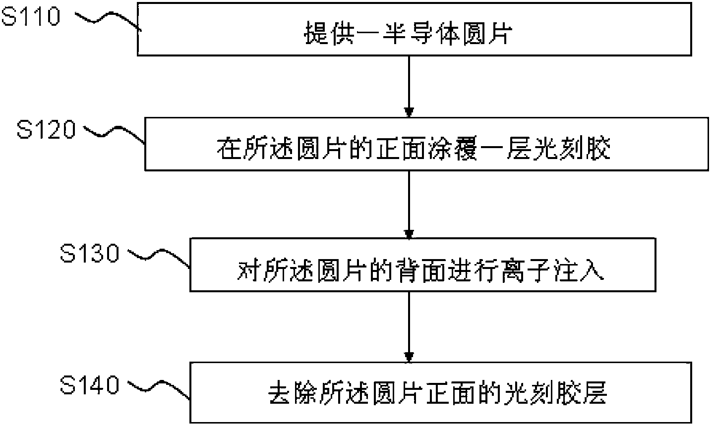
[0022] see figure 1 , which is a process flow diagram of the method of the present invention. Such as figure 1 As shown, the present invention is a method for protecting the front side of a semiconductor wafer when the back side is injected, which is to protect the front side by coating a layer of protective glue on the fr...


PUM

PropertyMeasurementUnit
Thicknessaaaaaaaaaa
Thicknessaaaaaaaaaa

Abstract

The invention provides a method for front face protection in back face implantation of a semiconductor wafer. A front face of the wafer is coated with a layer of photoresist before a semiconductor wafer back face manufacturing process is carried out, and the photoresist is removed after the back face manufacturing process is finished. The method specifically includes the steps: step one, providing the semiconductor wafer; step two, coating the photoresist layer onto the front face of the wafer; step three, subjecting the back face of the wafer to ion implantation; step four, removing the photoresist layer on the front face of the wafer. Compared with the prior art, the method for front face protection in back face implantation of the semiconductor wafer has the advantages that protection of a front face structure is realized by coating the front face of the semiconductor wafer with the photoresist before the semiconductor wafer is subjected to back face implantation; the method is simple, easy to implement and effective in protection, yield of semiconductor power devices is increased, and production cost is reduced.

Description

technical field [0001] The invention relates to the field of semiconductor manufacturing, in particular to a method for protecting the front side of a semiconductor wafer during injection into the back side. Background technique [0002] In the production process of semiconductor power devices, many processes involve the backside injection process. At this time, the wafer needs to be turned over for injection. When the implanter injects, the front structure is in contact with the equipment, which can easily lead to scratches on the front structure and product failure. , so that the wafer is scrapped, which not only wastes resources, but also increases production costs. At present, the general process is to grow a layer of oxide layer dielectric or SiN (silicon nitride) as a protective layer on the front to protect the front. After the back injection process is completed, the protective layer grown on the front is removed by etching. However, in the prior art, the method of ...

Claims


Application Information

Patent Timeline
IPC IPC(8): H01L21/265
CPCH01L21/265H01L21/26506
Inventor 芮强张硕王根毅邓小社
Owner CSMC TECH FAB1
Why Eureka
Try Eureka