Three-dimensional semiconductor memory device based on deep hole filling and preparation method thereof

A semiconductor and memory technology, which is applied in the field of three-dimensional semiconductor memory based on deep hole filling and its preparation, can solve the problems of deep holes being easily covered by deposited materials, uneven deposition of deep holes, and hindering the continued deposition of deep holes, etc. Increased density, high storage density, the effect of increasing storage density

Active Publication Date: 2015-01-07
HUAZHONG UNIV OF SCI & TECH
View PDF4 Cites 14 Cited by
  • Summary
  • Abstract
  • Description
  • Claims
  • Application Information

AI Technical Summary

Problems solved by technology

[0004] However, further studies have shown that the above-mentioned existing solutions still have the following technical problems: in order to prepare three-dimensional memory devices with a large number of devices in the vertical direction and a small area of ​​a single device, deep holes with high aspect ratio are often required in the preparation process, but are subject to Due to the limitations of the current deposition process, the deposition of deep holes is often uneven in the upper and lower parts, and because the upper part of the deep holes is easily covered by deposited materials during the deposition process, which hinders the continued deposition of the deep holes, affecting the stability of the device and production yield.

Method used


Image

  • Three-dimensional semiconductor memory device based on deep hole filling and preparation method thereof
  • Three-dimensional semiconductor memory device based on deep hole filling and preparation method thereof
  • Three-dimensional semiconductor memory device based on deep hole filling and preparation method thereof

Examples


Embodiment 1

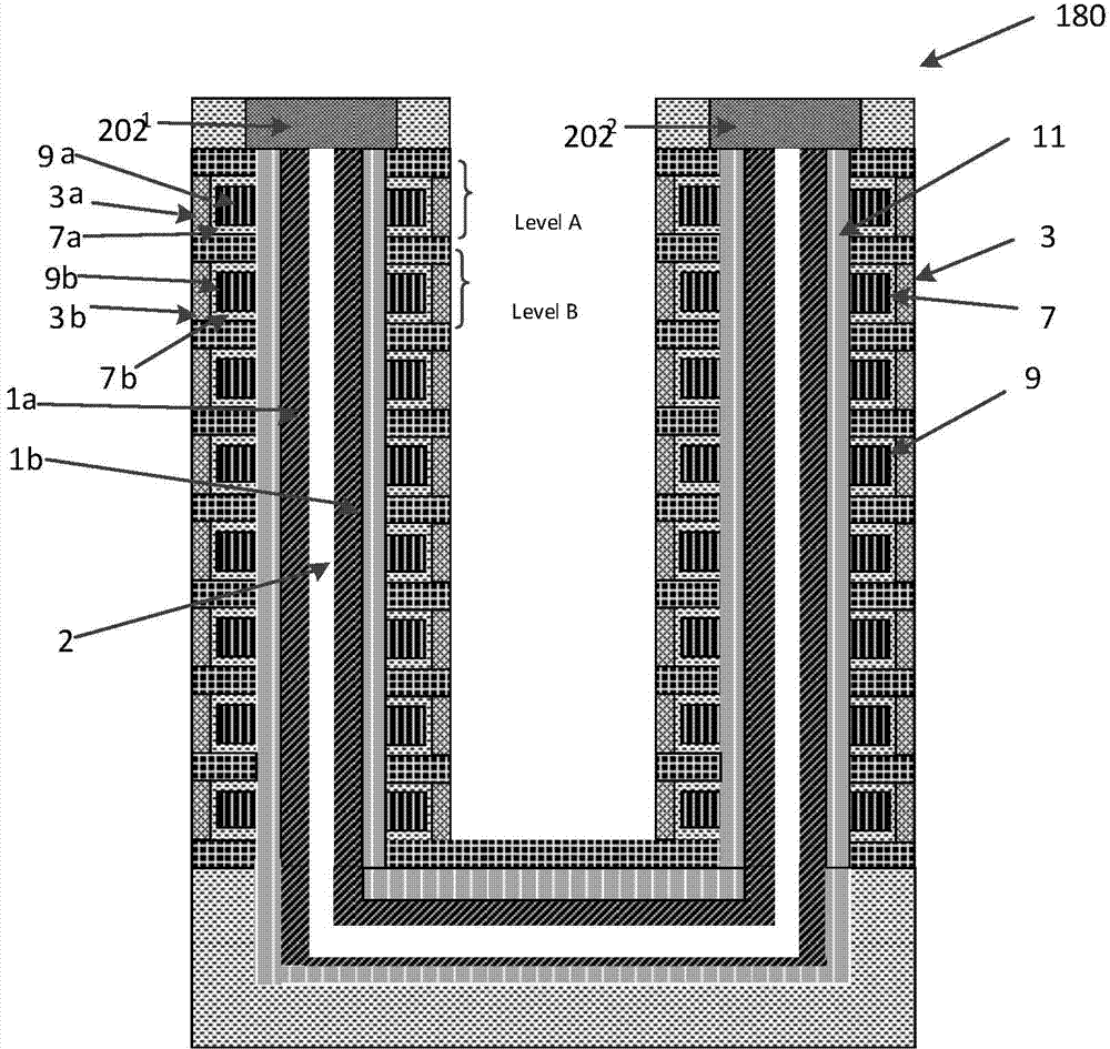
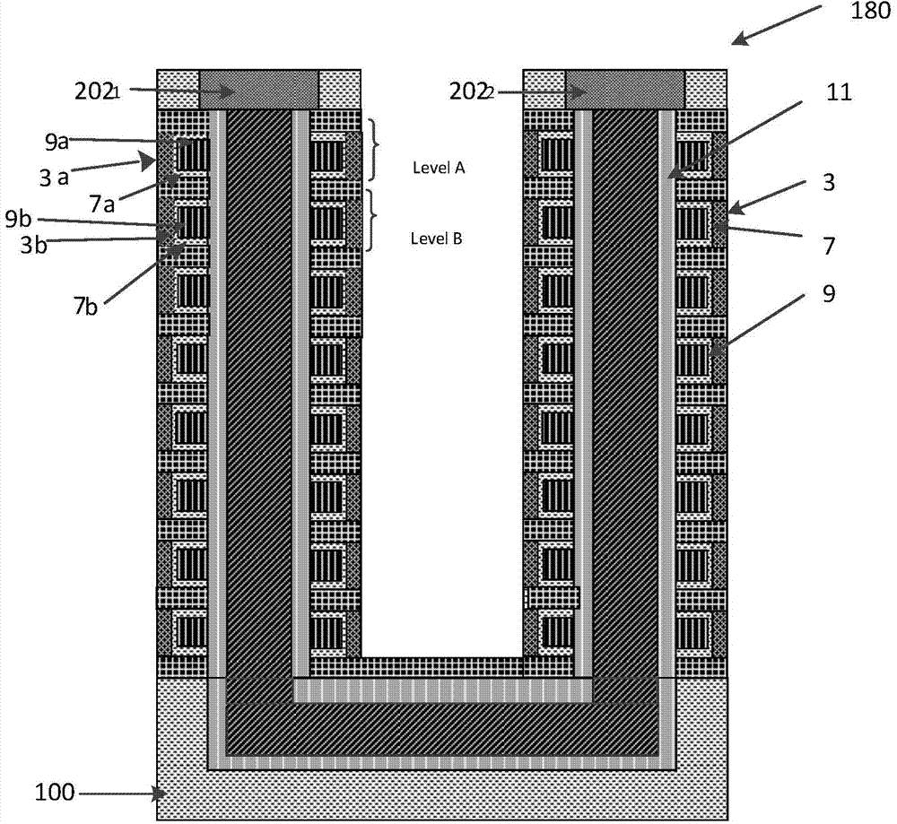
[0033] The source / drain of the NAND string is formed on the semiconductor channel 1 and as figure 1 and 2 As shown, channel 1 is U-shaped. Contact electrode 202 (including 202 1 、202 2 ) provides contact with the semiconductor channel 1 . The shape of the U-shaped tube in this paper is similar to the English letter "U". The electrodes of the U-shaped channel semiconductor storage device are drawn from the top of the device, which reduces the contact area of ​​the electrode; at the same time, the NAND string of the U-shaped semiconductor storage device can include a stacked structure in which at least one semiconductor layer and an insulating layer are alternately stacked, increasing The number of devices per unit area is increased, so the U-shaped channel semiconductor memory can greatly increase the storage density.

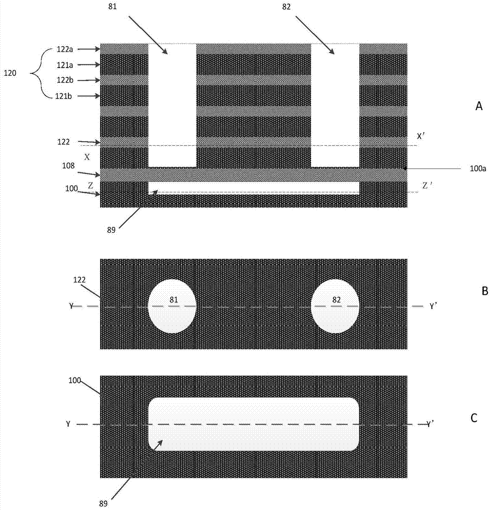
[0034] Combine below Figure 3-14 , specifically describe the process of preparing U-shaped semiconductor channel NAND strings.

[0035] (1) Form a sacr...


PUM


Abstract

The invention discloses a three-dimensional semiconductor memory device based on deep hole filling and a preparation method of the three-dimensional semiconductor memory device. The preparation method is suitable for preparing a U-shaped channel of the three-dimensional semiconductor memory device. The double-ion-beam deposition technology is adopted, a target material is bombarded with one beam of ions, molecules of the target material overflow and are deposited in a deep hole along a trail, the surface of the deep hole is bombarded with the other beam of ions, the deposited material can not cover the top of the deep hole, and therefore it is guaranteed that the U-shaped channel of the three-dimensional semiconductor memory device is completely formed. Electrodes of the three-dimensional semiconductor memory device with the U-shaped channel are led out from the upper side of the device, so that the electrode contact area is reduced; meanwhile, an NAND string of the U-shaped three-dimensional semiconductor memory device can comprise a stacking structure formed by alternately stacking at least one layer of semiconductors and an insulation layer, the number of devices in the unit area is increased, and therefore the memory density of the three-dimensional semiconductor memory device with the U-shaped channel can be greatly increased.

Description

technical field [0001] The invention belongs to the technical field of microelectronic devices and memory, and more specifically relates to a three-dimensional semiconductor memory based on deep hole filling and a preparation method thereof. Background technique [0002] Although polysilicon floating-gate non-volatile memory (NVM) arrays have achieved great success using 20nm (or less) semiconductor fabrication technology, further scaling has become very difficult. There are several reasons for this: crosstalk from adjacent cells and a small amount of programmable electrons in the floating gate. This limitation complicates multi-level storage with floating gates. Therefore, the development of three-dimensional memory devices is imperative. [0003] Especially in the field of embedded memory, three-dimensional back-end (B / E) nonvolatile memory arrays are also challenging because this approach allows for larger nonvolatile arrays. The use of large-capacity (>1Gbit) embed...

Claims


Application Information

Patent Timeline
Patent Type & Authority Applications(China)
IPC IPC(8): H01L27/115H01L21/8247H01L21/71
Inventor 缪向水季宏凯童浩
Owner HUAZHONG UNIV OF SCI & TECH
Why Eureka
Try Eureka