Method for forming contact hole with high aspect ratio

A high aspect ratio, contact hole technology, applied in electrical components, transistors, circuits, etc., can solve problems such as reducing production capacity and efficiency, increasing process cycle, etc., to improve performance, increase conduction speed, and reduce RC resistance The effect of

Active Publication Date: 2021-06-01
CHANGXIN MEMORY TECH INC
View PDF8 Cites 1 Cited by
  • Summary
  • Abstract
  • Description
  • Claims
  • Application Information

AI Technical Summary

Problems solved by technology

[0009] It can be seen that the etching-filling-etching-refilling (etch-dep-etch-dep) method is used in the prior art to avoid the influence of the bow-shaped bending of the sidewall of the contact hole on the filling of the conductive material, but this method increases the The process cycle reduces production capacity and efficiency, and it is necessary to optimize the process to improve production efficiency

Method used


Image

  • Method for forming contact hole with high aspect ratio
  • Method for forming contact hole with high aspect ratio
  • Method for forming contact hole with high aspect ratio

Examples


Embodiment Construction

[0026] The specific implementation of the method for forming a high aspect ratio contact hole provided by the present invention will be described in detail below in conjunction with the accompanying drawings.

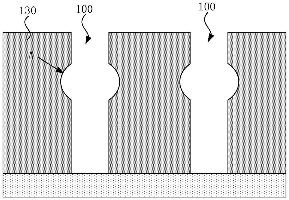
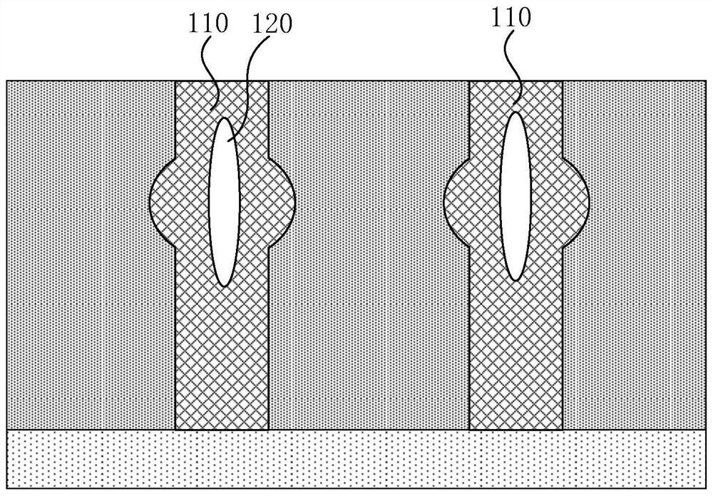
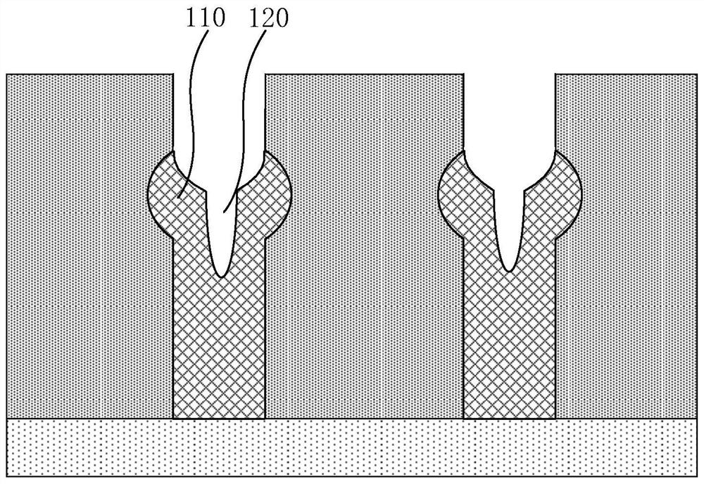
[0027] figure 2 is a schematic diagram of the steps of a specific embodiment of the method for forming a high aspect ratio contact hole of the present invention, please refer to figure 2 The method for forming a contact hole with a high aspect ratio of the present invention comprises the following steps: step S20, providing a substrate; step S21, forming a dielectric layer on the substrate, the dielectric layer including a non-over-etching region and an easy-over-etching region. etching area, and the dielectric layer includes at least two sub-dielectric layers and an auxiliary layer located between the sub-dielectric layers, the auxiliary layer is located in the easily overetched area, and the sub-dielectric layer is located in the In the non-overetched region, the e...


PUM

PropertyMeasurementUnit
heightaaaaaaaaaa
thicknessaaaaaaaaaa

Abstract

The invention provides a method for forming a contact hole with a high aspect ratio, which comprises the following steps that a substrate is provided, a dielectric layer is formed on the substrate, the dielectric layer comprises a non-easy over-etching region and an easy over-etching region, the dielectric layer comprises at least two sub-dielectric layers, an auxiliary layer is arranged between the sub-dielectric layers and located in the easy over-etching region, the sub-dielectric layer is located in a non-easy over-etching region, and the etching rate of the etching substance to the auxiliary layer is smaller than the etching rate of the etching substance to the dielectric layer; a patterned mask layer is formed on the dielectric layer, the mask layer is provided with a pattern window, and the pattern window exposes the dielectric layer; and the dielectric layer and the auxiliary layer are etched by taking the mask layer as a barrier layer to form the contact hole with the high aspect ratio. The method has the advantages that the auxiliary layer is added in the easy over-etching region of the dielectric layer, so that the resistance of the region to plasma bombardment is enhanced, the region cannot be over-etched by plasma, the subsequent filling of a conductive material cannot be influenced, and the performance of the device is greatly improved.

Description

technical field [0001] The invention relates to the field of semiconductor manufacturing, in particular to a method for forming a contact hole with a high aspect ratio. Background technique [0002] Dynamic Random Access Memory (English: Dynamic Random Access Memory, DRAM for short) is a semiconductor memory widely used in multi-computer systems. The DRAM structure includes transistors, word lines, bit lines, capacitors, metal interconnects, and peripheral regions. [0003] With the improvement of the integration level of the semiconductor process, the line width of the device will be further reduced, and the aspect ratio of the contact hole in the semiconductor process will continue to increase. When making high-aspect-ratio contact holes, the sidewall (profile) will appear bow-shaped (bow), and cause the bottom critical dimension (bottom CD) to be small, which will affect the filling of conductive materials in subsequent contact holes, increase RC delay, and affect devic...

Claims


Application Information

Patent Timeline
Patent Type & Authority Applications(China)
IPC IPC(8): H01L21/768H01L27/108
CPCH01L21/76802H01L21/76829H10B12/00
Inventor 赵哲
Owner CHANGXIN MEMORY TECH INC
Why Eureka
Try Eureka