Manufacturing method of semiconductor device shallow-trench isolation structure
A technology of isolation structure and manufacturing method, which is applied in semiconductor/solid-state device manufacturing, electrical components, circuits, etc., can solve the problems that the STI isolation structure is difficult to further shrink and affect device performance, etc., to reduce width, increase area, and improve integration degree of effect
- Summary
- Abstract
- Description
- Claims
- Application Information
AI Technical Summary
Problems solved by technology
Method used
Image

Examples
Embodiment 1
[0045] Such as Figure 6 and Figure 8 ~ Figure 14 As shown, this embodiment provides a method for manufacturing a shallow trench isolation structure of a semiconductor device, including the following steps:
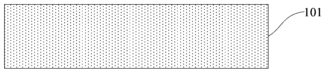
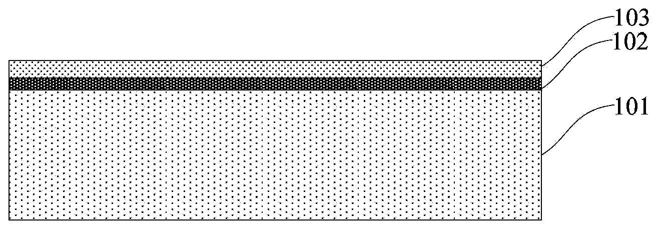
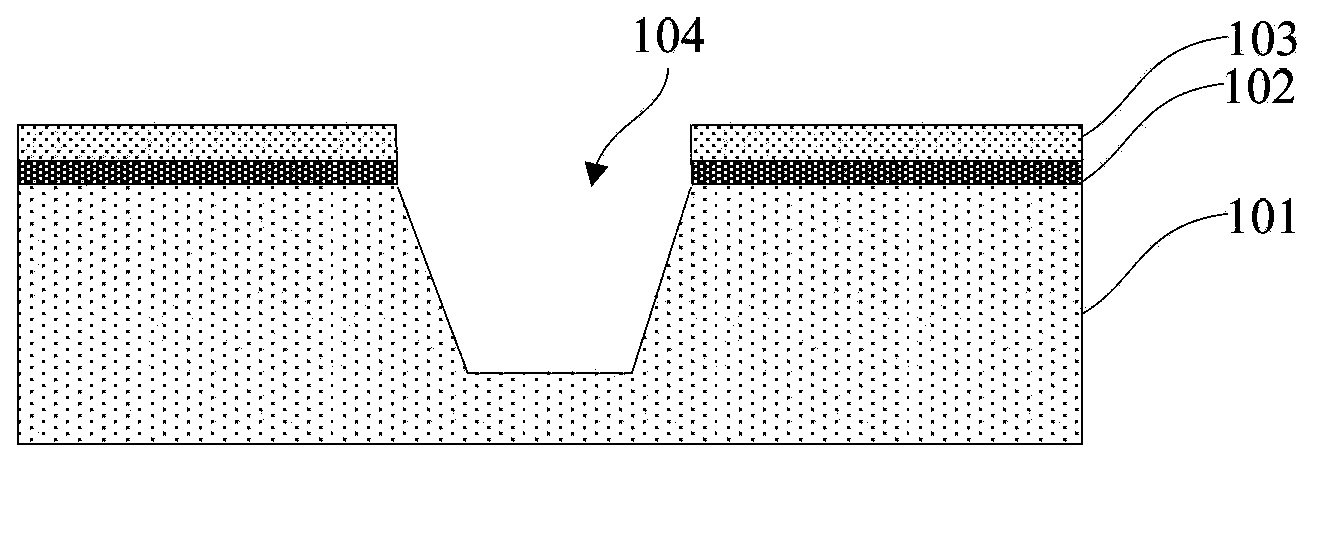
[0046] Such as Figure 6 and Figure 8 ~ Figure 10 As shown, step 1) S11 is first performed, providing a silicon substrate 201, forming a mask layer on the surface of the silicon substrate 201, and forming shallow trenches 204 in the silicon substrate 201 by photolithography.
[0047] As an example, the mask layer is a stack of silicon dioxide layer 202 and silicon nitride layer 203, and its thickness is 30 nm˜200 nm. Of course, in other embodiments, other materials such as high-k dielectric materials can also be used as the mask layer.
[0048] Specifically, in this step, a photoresist (not shown) is formed on the surface of the mask layer, and then an etching window is formed by exposure, and the silicon substrate 201 under the etching window is etched to form a sh...
Embodiment 2
[0059] Such as Figure 7 ~ Figure 15 As shown, this embodiment provides a method for manufacturing a shallow trench isolation structure of a semiconductor device, including the following steps:
[0060] Such as Figure 7 ~ Figure 10 As shown, step 1) S21 is first performed, providing a silicon substrate 201, forming a mask layer on the surface of the silicon substrate 201, and forming shallow trenches 204 in the silicon substrate 201 by photolithography.
[0061] As an example, the mask layer is a stack of silicon dioxide layer 202 and silicon nitride layer 203, and its thickness is 30 nm˜200 nm. Of course, in other embodiments, other materials such as high-k dielectric materials can also be used as the mask layer.
[0062] Specifically, in this step, a photoresist (not shown) is formed on the surface of the mask layer, and then an etching window is formed by exposure, and the silicon substrate 201 under the etching window is etched to form a shallow trench groove 204 . In...
PUM
| Property | Measurement | Unit |
|---|---|---|
| Thickness | aaaaa | aaaaa |
| Thickness | aaaaa | aaaaa |
| Thickness | aaaaa | aaaaa |
Abstract
Description
Claims
Application Information
PatSnap Eureka turns technology decisions into work you can execute. Powered by our Innovation Knowledge Graph, it runs expert workflows across engineering, life sciences, materials and intellectual property. Get your review-ready output in minutes.


