Improved optional grid driving circuit

A driving circuit and selection gate technology, applied in information storage, static memory, instruments, etc., can solve the problems affecting circuit performance, memory reading speed, affecting the speed of SG voltage drop, etc., to speed up the discharge speed, provide reading The effect of taking performance and improving overall performance

Inactive Publication Date: 2015-01-21
SUZHOU KUANWEN ELECTRONICS SCI & TECH
View PDF6 Cites 0 Cited by
  • Summary
  • Abstract
  • Description
  • Claims
  • Application Information

AI Technical Summary

Problems solved by technology

The 2-T structure has strong anti-bit line crosstalk ability, good programming and erasing stability, and is generally suitable for occasions with strict requirements on voltage and power consumption, but low capacity and low density
When reading the state, the SG terminal should output the negative low voltage provided by the voltage input port VNNSG, while the WELL and VPPSG terminals should output high level vdd. After XD becomes high level, the M4 tube is turned off, and SG drops from vdd to Negative low voltage, because the M6 ​​tube is not turned off all the time, the voltage at the SGB terminal is unstable, which affects the speed of the SG voltage drop and affects the overall read speed of the memory
In the erasing state, the CHIPERASE terminal is connected to a high level vdd, causing the M5 tube to be turned off, and the SGB node (the gate of the M7 tube) to float, which affects the performance of the circuit and easily causes the SG terminal to output a wrong voltage.

Method used


Image

  • Improved optional grid driving circuit
  • Improved optional grid driving circuit
  • Improved optional grid driving circuit

Examples


Embodiment Construction

[0028] The present invention will be described in detail below with reference to the accompanying drawings and in combination with embodiments.

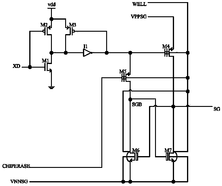
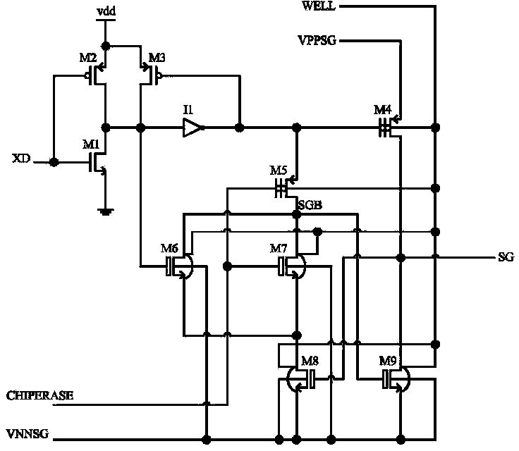
[0029] Such as image 3 As shown, an improved selection gate drive circuit includes a first signal terminal WELL, a second signal terminal VPPSG, a third signal terminal CHIPERASE, a fourth signal terminal VNNSG, a decoder output terminal XD and a signal output terminal SG.

[0030] Wherein, the gate of the first NMOS transistor M1 is connected to the decoder output signal XD, the source of the first NMOS transistor M1 is grounded, the drain of the first NMOS transistor M1 is connected to the drain of the first PMOS transistor M2, and the first PMOS The gate of the transistor M2 is connected to the decoder output signal XD, and the source of the first PMOS transistor M2 is connected to the power supply voltage vdd. The gate of the second PMOS transistor M3 is connected to the output terminal of the first inverter I1, the source of t...


PUM


Abstract

The invention discloses an improved optional grid driving circuit. Compared with the conventional optional grid driving circuit, the circuit is characterized in that two NMOS transistors of triple-well process are additionally arranged, wherein an NMOS transistor (a second NMOS tube M6) is capable of isolating during reading; the other NMOS transistor (a third NMOS tube M7) is capable of avoiding flotation node in the circuit during wiping. The optional grid driving circuit is relatively short in response time during reading, so that the reading is accelerated; the reading period is shortened; the influence of the flotation node is avoided during wiping; the hidden danger of error circuit function is avoided; the overall stability of a memorizer is improved; the access performance of the memorizer is improved.

Description

technical field [0001] The invention relates to the field of Flash memory, in particular to a selection gate driving circuit of a multi-gate memory. Background technique [0002] In recent years, non-volatile memory has been used in a large number of different kinds of applications such as code and data storage. In particular, Flash memory is widely used in portable applications for storing images, sound, music, video, and the like. The most classic structure of Flash memory is the ETOX single-tube structure proposed by Intel Corporation, which effectively reduces the area of ​​the storage unit, but brings a series of problems such as over-erasing and bit line crosstalk, which is different from the single-tube Flash structure. 2 The -T Flash structure adopts a structure in which the storage tube and the selection tube are connected in series, and the storage cells in the array that do not need to be accessed are completely turned off through the selection tube. The 2-T str...

Claims


Application Information

Patent Timeline
Patent Type & Authority Applications(China)
IPC IPC(8): G11C16/14G11C16/26G11C16/34
Inventor 翁宇飞李力南姜伟李二亮胡玉青
Owner SUZHOU KUANWEN ELECTRONICS SCI & TECH
Why Eureka
Try Eureka