Eureka AIR delivers breakthrough ideas for toughest innovation challenges, trusted by R&D personnel around the world.

Method for manufacturing gallium arsenide laser capable of lowering electron leakage

A technology of electron leakage and manufacturing method, which is applied in the direction of lasers, phonon exciters, laser components, etc., can solve problems such as electron leakage, and achieve the effect of reducing electron leakage

Active Publication Date: 2015-01-21
INST OF SEMICONDUCTORS - CHINESE ACAD OF SCI
View PDF4 Cites 0 Cited by
  • Summary
  • Abstract
  • Description
  • Claims
  • Application Information

AI Technical Summary

Problems solved by technology

Second, the carriers trapped by the quantum well escape again due to the higher temperature of the active region, resulting in electron leakage
Third, the electrons and holes captured by the quantum well recombine, but the energy released by the recombination is not released in the form of photons, but is transferred to the adjacent electrons or holes to become hot carriers, resulting in electron leakage

Method used


Image

  • Method for manufacturing gallium arsenide laser capable of lowering electron leakage
  • Method for manufacturing gallium arsenide laser capable of lowering electron leakage

Examples


Embodiment Construction

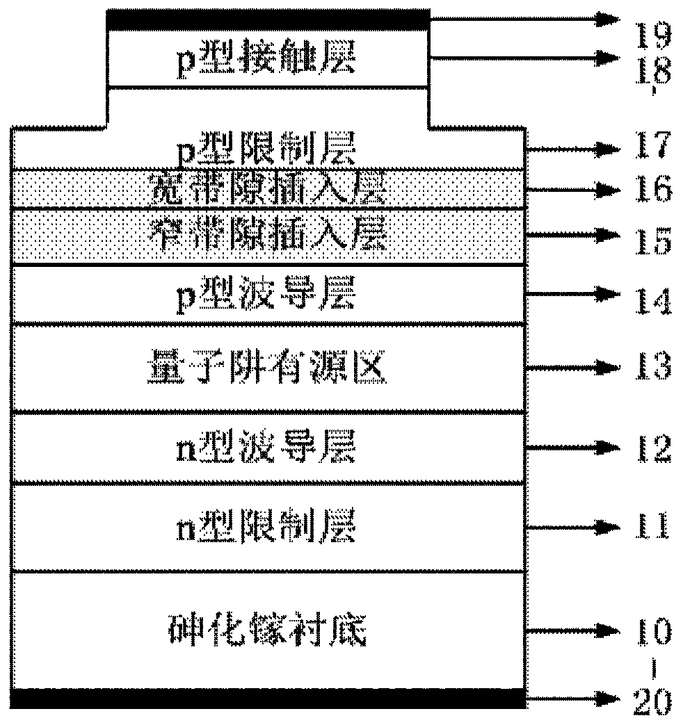
[0017] see figure 1 As shown, the present invention provides a method for manufacturing a gallium arsenide laser with reduced electron leakage, which includes the following steps.

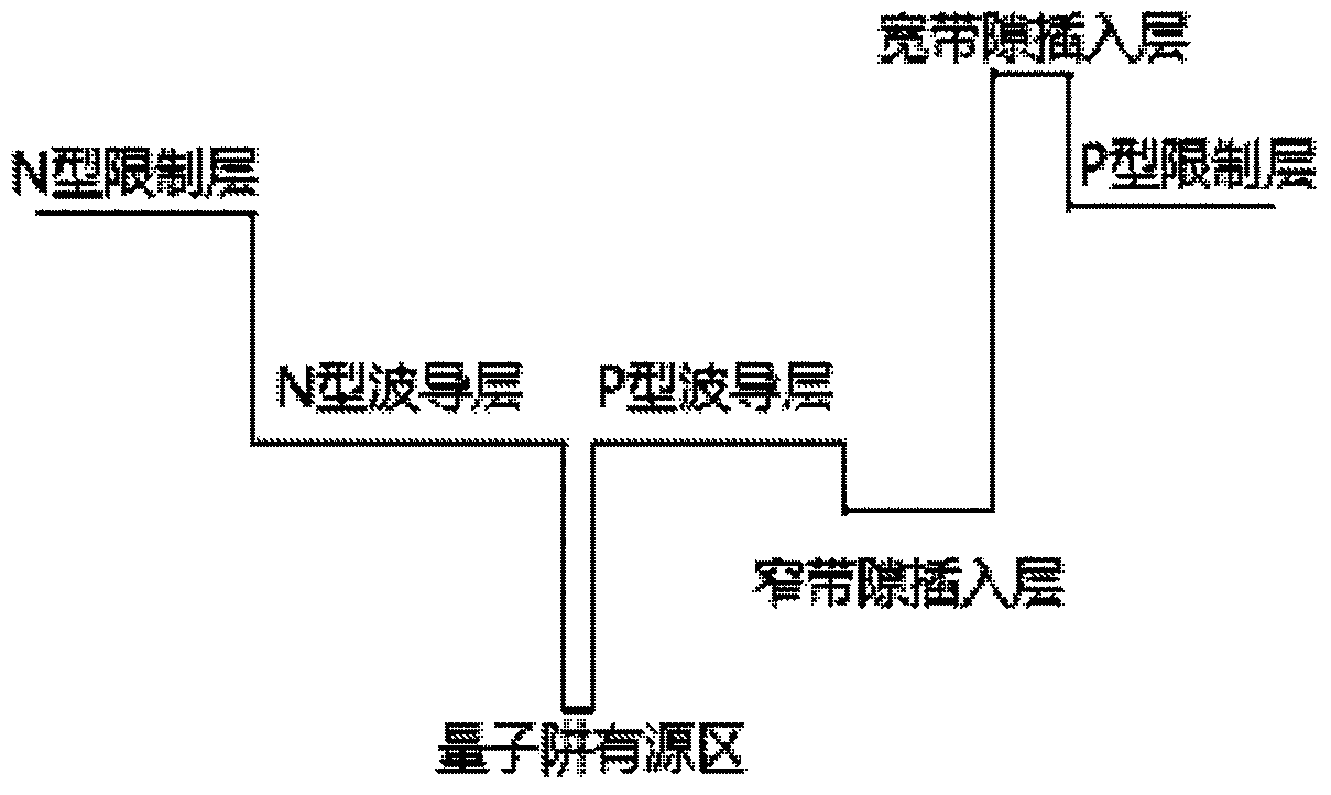
[0018] Step 1: Epitaxially grow N-type confinement layer 11, N-type waveguide layer 12, quantum well active region 13, P-type waveguide layer 14, narrow-bandgap insertion layer 15, wide-bandgap insertion layer 16, P-type confinement layer 17 and P-type contact layer 18 .

[0019] Step 2: Etch the P-type contact layer 18 and the P-type confinement layer 17 into a ridge shape by wet etching or dry etching. The wet etching operation is relatively simple and can be used when the etching depth is not very deep, but it is easy to cause undercutting and has a great impact on the device. If the corrosion depth is very deep, it is best to use dry etching such as ICP.

[0020] Step 3: growing a layer of oxide mold on the ridge-shaped surface, and using photolithography to form a P-type ohmic electrode 19 ...


PUM

PropertyMeasurementUnit
Thicknessaaaaaaaaaa
Thicknessaaaaaaaaaa
Thicknessaaaaaaaaaa

Abstract

Provided is a method for manufacturing a gallium arsenide laser capable of lowering electron leakage. The method comprises the following steps that (1) an N-type constraint layer, an N-type waveguide layer, a quantum well active region, a P-type waveguide layer, a narrow band gap insertion layer, a broad band gap insertion layer, a P-type restriction layer and a P-type contact layer are formed on a gallium arsenide substrate in sequence in an epitaxial growth mode; (2) the P-type contact layer and the P-type restriction layer are etched into a ridge shape by adopting a wet etching method or a dry etching method; (3) a P-type ohmic electrode is manufactured on the upper surface of the P-type restriction layer; (4) the gallium arsenide substrate is thinned and cleaned; (5) an N-type ohmic electrode is manufactured on the backface of the gallium arsenide substrate so that the laser is formed; (6) cleavage is carried out, the cavity surface of the laser is coated with a film, finally the laser is encapsulated on a tube, and manufacturing is completed. According to the method for manufacturing the gallium arsenide laser, electron leakage can be lowered greatly.

Description

technical field [0001] The invention relates to the technical field of semiconductor optoelectronic devices, and relates to a method for manufacturing a gallium arsenide laser that reduces electron leakage. Background technique [0002] With the rapid development of semiconductor optoelectronic devices, high-power semiconductor lasers came into being. Due to the advantages of small size, low price, high electro-optical conversion efficiency and long life of semiconductor lasers, semiconductor lasers have a very wide range of applications in the field of optoelectronics. Semiconductor lasers play an important role in the fields of industrial processing, medical treatment, military and theoretical research. Gallium arsenide is the most well-studied material so far compared to other semiconductor III-V materials. Therefore, people have the highest performance requirements for gallium arsenide lasers. This is reflected in the fact that gallium arsenide lasers can have very low...

Claims


Application Information

Patent Timeline
IPC IPC(8): H01S5/343
Inventor 李翔赵德刚江德生刘宗顺陈平朱建军
Owner INST OF SEMICONDUCTORS - CHINESE ACAD OF SCI
Why Eureka
Eureka Blog
Learn More