Through silicon via process

A through-silicon hole and process technology, applied in the direction of electrical components, semiconductor/solid-state device manufacturing, circuits, etc., can solve the problem of destroying semiconductor devices

Active Publication Date: 2015-01-28
WUHAN XINXIN SEMICON MFG CO LTD
View PDF4 Cites 23 Cited by
  • Summary
  • Abstract
  • Description
  • Claims
  • Application Information

AI Technical Summary

Problems solved by technology

[0003] However, this technology uses the first wafer metal as a barrier layer in the process of contacting circuits on different wafers in the same area to realize metal interconnection between wafers during the second etching process to form TSVs. Time charged particles bombard the first BEOL dielectric layer (Back-End-Of-Line, referred to as BEOL, also known as the back-end process layer) (in the present invention, the bonded wafer at the top is referred to as the first A wafer, and the metal in the BEOL dielectric layer of the first wafer is called the first BEOL dielectric layer) causes a large amount of charge to accumulate in the metal in the first BEOL dielectric layer, thereby destroying the semiconductor device in the first BEOL dielectric layer

Method used


Image

  • Through silicon via process
  • Through silicon via process
  • Through silicon via process

Examples


Embodiment Construction

[0023] The present invention will be further described below in conjunction with the accompanying drawings and specific embodiments, but not as a limitation of the present invention.

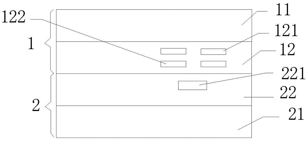
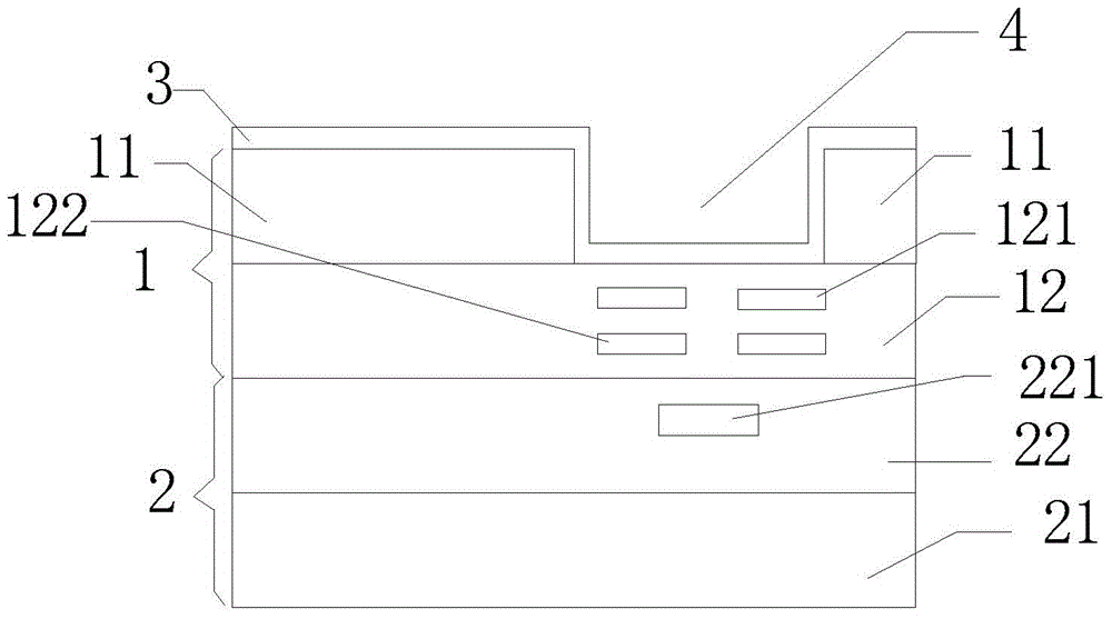
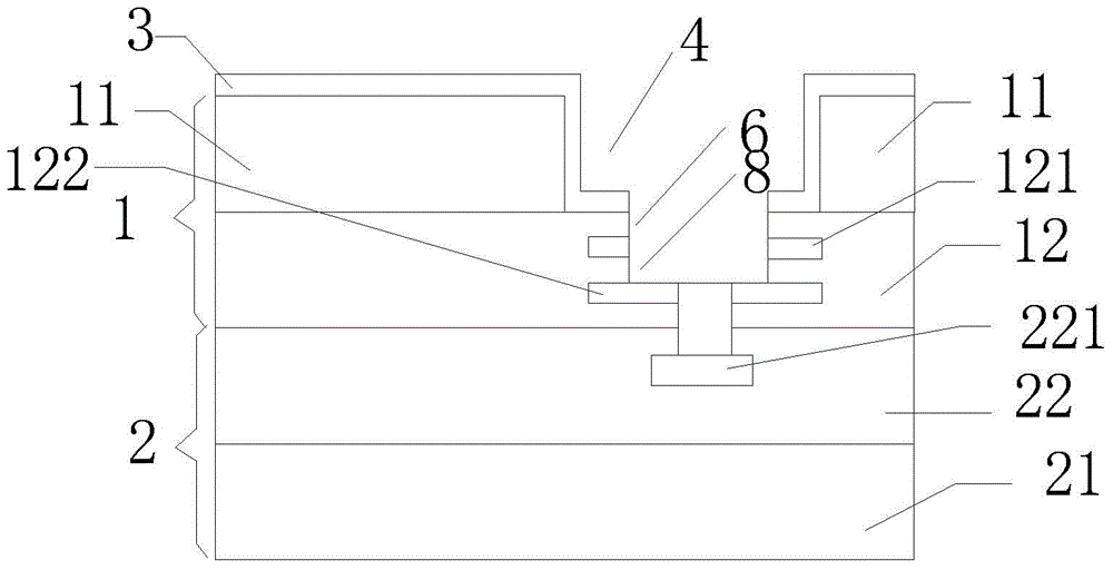
[0024] In view of the above existing problems, the present invention discloses a through-silicon via process, which effectively solves the damage of semiconductor devices caused by charge accumulation in the cross-wafer through-silicon via interconnection process. Part of the second metal layer contained in the first BEOL dielectric layer and part of the third metal layer contained in the second BEOL dielectric layer are connected to the semiconductor device, so that the chip is reduced in size without affecting performance, and the traditional three-dimensional wafer is completed. Integration; at the same time, part of the first metal layer contained in the first BEOL dielectric layer is not connected to any device to achieve the effect of grounding, which can overcome the long-term bombardment ...


PUM


Abstract

The invention belongs to the semiconductor manufacturing technical field and relates to a through silicon via process. The through silicon via process includes the following steps that: traditional wafer three-dimensional integration is performed on a part of a second metal layer contained in a first BEOL dielectric layer and a third metal layer contained in a second BEOL dielectric layer, so that the size of a wafer can be reduced greatly with the properties of the wafer unchanged; and a part of a first metal layer contained in the first BEOL dielectric layer is not connected with any circuit, and therefore, accumulation of a large number of charges in first wafer metal which is caused by long-term bombardment of charged particles to metal in the first BEOL dielectric layer in secondary etching in a traditional process can be avoided, and damage to a semiconductor device in the first BEOL dielectric layer can be avoided.

Description

technical field [0001] The invention relates to the technical field of semiconductor manufacturing, in particular to a through-silicon via process. Background technique [0002] With the miniaturization and thinning of electronic devices and memories, there are higher requirements for the volume and thickness of chips. The three-dimensional integration of wafers is an effective solution to reduce the volume and thickness of chips. This technology integrates two or more chips with the same or different functions through bonding. This integration increases the size of the chip while maintaining the chip volume. The scale improves the performance of the chip, no longer limited by the manufacturing process of a single chip, and also shortens the metal interconnection between functional chips, which greatly reduces heat generation, power consumption, and delay; at the same time, it greatly improves the bandwidth between functional modules , such as the three-dimensional integrat...

Claims


Application Information

Patent Timeline
Patent Type & Authority Applications(China)
IPC IPC(8): H01L21/768
CPCH01L21/76877
Inventor 董金文朱继锋肖胜安胡思平
Owner WUHAN XINXIN SEMICON MFG CO LTD
Why Eureka
Try Eureka