Method for forming air gaps among copper interconnection lines

An air-gap, copper interconnect technology, applied in electrical components, semiconductor/solid-state device manufacturing, circuits, etc., can solve problems such as copper wire over-etching, corrosion of copper interconnect wires, collapse, etc., to reduce process requirements, improve Product yield and the effect of improving controllability

Inactive Publication Date: 2015-01-28
SHANGHAI INTEGRATED CIRCUIT RES & DEV CENT
View PDF3 Cites 5 Cited by
  • Summary
  • Abstract
  • Description
  • Claims
  • Application Information

AI Technical Summary

Problems solved by technology

However, since the copper seed layer cannot be etched by dry method, the etching process of the seed layer and the barrier layer generally adopts a wet etching process in this process, which will corrode the sidewall of the copper interconnection line and cause copper interconnection It is difficult to control the key dimension of the wire. In addition, it is easy to cause the problem of over-etching at the bottom of the copper wire (Undercut), causing the copper wire to tilt or collapse
This integration scheme is difficult to achieve an air-gap process with extremely small critical dimensions

Method used


Image

  • Method for forming air gaps among copper interconnection lines
  • Method for forming air gaps among copper interconnection lines
  • Method for forming air gaps among copper interconnection lines

Examples


Embodiment Construction

[0038] In order to make the content of the present invention clearer and easier to understand, the content of the present invention will be further described below in conjunction with the accompanying drawings. Of course, the present invention is not limited to this specific embodiment, and general replacements known to those skilled in the art are also covered within the protection scope of the present invention.

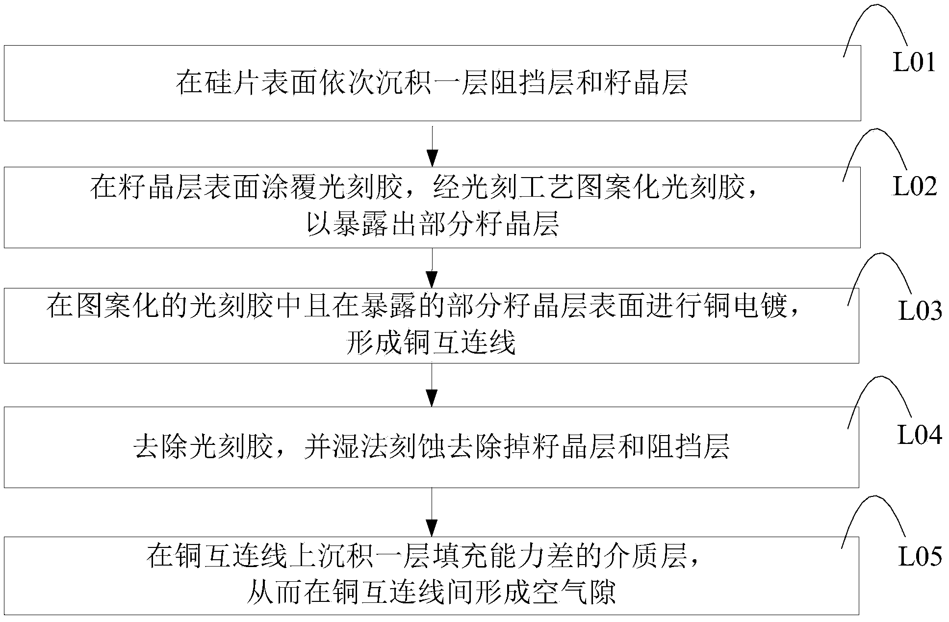
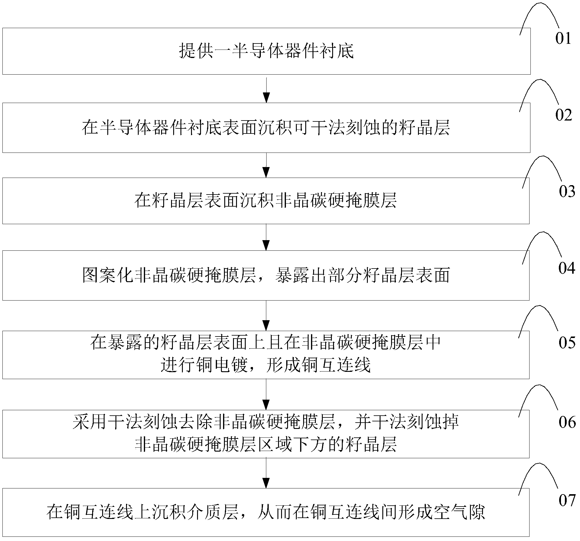
[0039] The following will be combined with Figure 2-9 The method for forming the air gap in the copper interconnection of the present invention will be further described in detail with specific embodiments. in, figure 2 is a schematic flow chart of a method for forming an air gap in a preferred embodiment of the present invention, Figure 3-9 It is a schematic diagram corresponding to each preparation step of the air gap forming method of a preferred embodiment of the present invention. It should be noted that the drawings are all in a very simplified form, us...


PUM


Abstract

The invention provides a method for forming air gaps among copper interconnection lines. The method for forming the air gaps among the copper interconnection lines comprises the steps of providing a semiconductor device substrate; depositing a seed crystal layer which can be subjected to dry etching on the surface of the semiconductor device substrate; depositing a hard amorphous carbon mask layer on the surface of the seed crystal layer; patterning the hard amorphous carbon mask layer to enable partial seed crystal layer surface to be exposed; conducting copper electroplating on the exposed seed crystal layer surface and in the hard amorphous carbon mask layer to form the copper interconnection lines; removing the hard amorphous carbon mask layer and the seed crystal layer under a hard amorphous carbon mask layer region through dry etching; depositing a dielectric layer on the copper interconnection lines and accordingly forming the air gaps among the copper interconnection lines. By means of the method for forming the air gaps among the copper interconnection lines, the high requirements of a photo-etching and etching technologies for continuous downscaling of key dimensions can be met, the problem of over etching of the bottoms of the copper interconnection lines, caused by a wet etching process and the problem that the key dimensions cannot be controlled are solved, the controllability of the key dimensions is improved, and the yield of products is improved.

Description

technical field [0001] The invention relates to the technical field of semiconductors, in particular to a method for forming an air gap between copper interconnecting lines. Background technique [0002] With the rapid development of electronic information technology, the replacement of consumer electronic products is becoming more and more frequent, which promotes the rapid development of integrated circuit manufacturing technology. As the critical dimensions of integrated circuits continue to shrink, technical problems continue to emerge. Among them, the RC delay of the copper interconnection has gradually become one of the important components of the RC delay of the entire chip, and cannot be ignored. [0003] The industry generally adopts lower dielectric constant (Low-k) dielectrics to reduce the RC delay of copper interconnect lines. In the 90nm to 65nm technology generation, the industry generally uses SiOCH dielectrics with a dielectric constant of 2.6 to 3.0, such...

Claims


Application Information

Patent Timeline
Patent Type & Authority Applications(China)
IPC IPC(8): H01L21/768
CPCH01L21/7682
Inventor 林宏
Owner SHANGHAI INTEGRATED CIRCUIT RES & DEV CENT
Why Eureka
Try Eureka