hdi printed circuit board high uniformity through-hole plating device

A printed circuit board, through-hole electroplating technology, applied in the direction of printed circuit, printed circuit manufacturing, printed component electrical connection formation, etc., can solve the problems that the concentration of the plating solution cannot be reasonably controlled, the plating layer is uneven, etc., and achieve the suppression of hydrogen evolution Side reactions, high cathode current efficiency, and efficiency-enhancing effects

Inactive Publication Date: 2017-05-24
ZHEJIANG ZHENYOU ELECTRONICS CO LTD
View PDF2 Cites 0 Cited by
  • Summary
  • Abstract
  • Description
  • Claims
  • Application Information

AI Technical Summary

Problems solved by technology

However, in this application, the concentration of the plating solution cannot be reasonably controlled, and the plating layer is not uniform

Method used


Image

  • hdi printed circuit board high uniformity through-hole plating device

Examples


Embodiment Construction

[0028] The following description is merely exemplary in nature and not intended to limit the disclosure, application or use. The specific implementation of the high-uniformity through-hole plating device for HDI printed circuit boards of the present invention will be further described below in conjunction with the accompanying drawings.

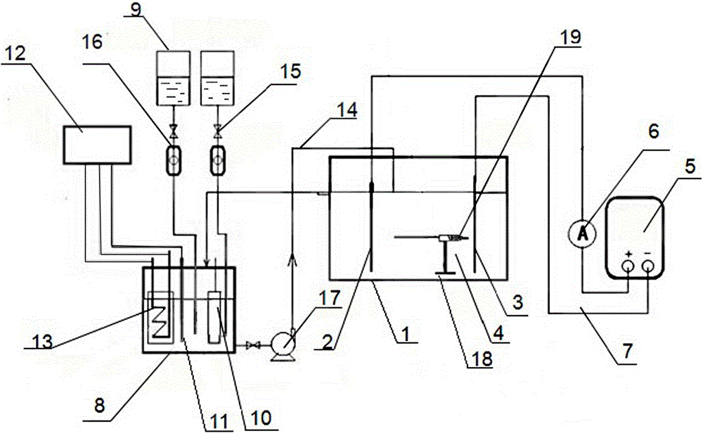
[0029] Such as figure 1 Shown is a schematic structural view of a preferred embodiment of the HDI printed circuit board high-uniformity through-hole plating device according to the present invention. The HDI printed circuit board high uniformity through-hole electroplating device according to the present invention comprises an electroplating tank 1, an anode 2, a cathode 3, a rectification power supply 5 and an ammeter 6, and the anode 2 and the cathode 3 are connected to the rectification power supply through a copper cable 7 5 is connected to the ammeter 6, and the electroplating tank 1 is provided with a spray mechanism 4. As the electro...


PUM


Abstract

The invention relates to the technical field of through hole processing of HDI (high density inverter) printed wiring boards and particularly relates to a high-uniformity electroplating device for through holes of an HDI (high density inverter) printed wiring board. The device comprises an electroplating bath (1), an anode (2), a cathode (3) and a rectifying power supply (5), wherein the electroplating bath (1) is internally provided with a spraying mechanism (4) which can move in the electroplating bath (1) to directionally spray the surfaces of the through holes of the HDI board at a high speed. The cathode deposition currents on the surfaces of the through holes of the HDI board obtained are uniformly distributed, the copper layers are continuously distributed and are uniform in thickness, compact in organization structure, and good in conductivity, and the plating quality is improved. By using the electroplating device, the cathode current efficiency in the electroplating device is high, the hydrogen evolution side reaction is better inhibited, the efficiency of the electroplating production process is improved and the influence of hydrogen evolution on the quality of the copper layers is reduced, thereby facilitating reduction of the production cost.

Description

technical field [0001] The invention relates to the technical field of through-hole processing of HDI printed circuit boards, in particular to a high-uniformity through-hole electroplating device for HDI printed circuit boards. Background technique [0002] With the continuous development of consumer electronics products such as smartphones and tablet computers towards portability and miniaturization, PCBs are constantly being developed towards higher and more dense layouts. There are mainly three types of through holes, blind holes, and buried holes in HDI boards. The diameter of the through hole is about 100-150 microns, and its depth depends on the number of layers of the HDI board, generally more than a few hundred microns. Through-holes are generally formed by mechanical drilling, and the metallization of through-holes is a very important link in the manufacture of HDI boards, which involves processes such as electroless plating and electroplating. The through-hole pl...

Claims


Application Information

Patent Timeline
Patent Type & Authority Patents(China)
IPC IPC(8): C25D5/08C25D21/12C25D21/10C25D19/00H05K3/42
CPCC25D5/08C25D21/10C25D21/12H05K3/423
Inventor 詹有根徐军洪傅持军潘青高云芳
Owner ZHEJIANG ZHENYOU ELECTRONICS CO LTD
Why Eureka
Try Eureka