Quantum light source chip based on optical superlattice and waveguide light path

A technology of optical superlattice and waveguide light, which is applied in the field of quantum information technology, optoelectronic technology and nonlinear optics. It can solve the problems of not being stable, not having the ability to expand functions, and being huge, so as to improve the production efficiency and fast and accurate photon phase. The effect of regulation

Active Publication Date: 2017-02-22
NANJING UNIV
View PDF5 Cites 0 Cited by
  • Summary
  • Abstract
  • Description
  • Claims
  • Application Information

AI Technical Summary

Problems solved by technology

[0003] However, whether it is a birefringent crystal, an optical superlattice bulk material or a waveguide structure, a crystal can only produce one kind of entangled light source, and many other optical elements are often needed before and after the nonlinear crystal to realize the pump light and generate The processing and collection of photon pairs, etc., lead to the generation of entangled light sources. The optical path is generally complex, large, not stable, and does not have good function expansion capabilities.

Method used


Image

  • Quantum light source chip based on optical superlattice and waveguide light path
  • Quantum light source chip based on optical superlattice and waveguide light path
  • Quantum light source chip based on optical superlattice and waveguide light path

Examples


Embodiment 1

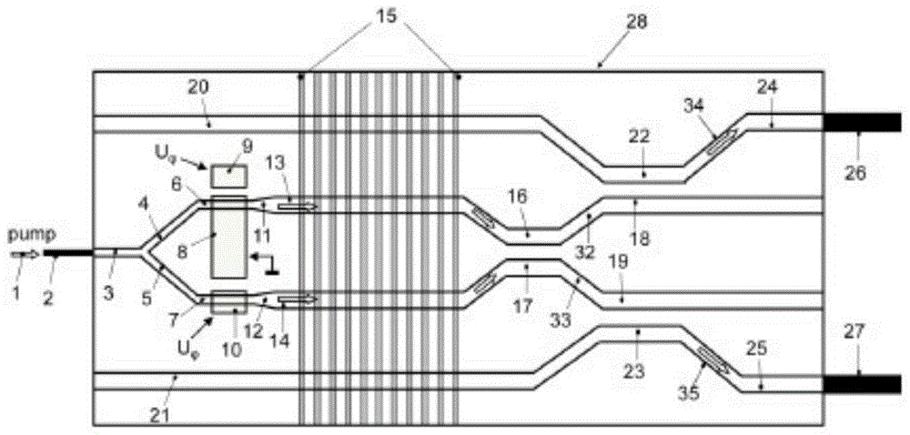
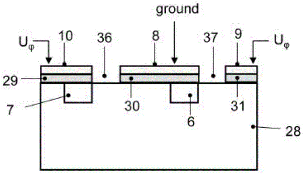
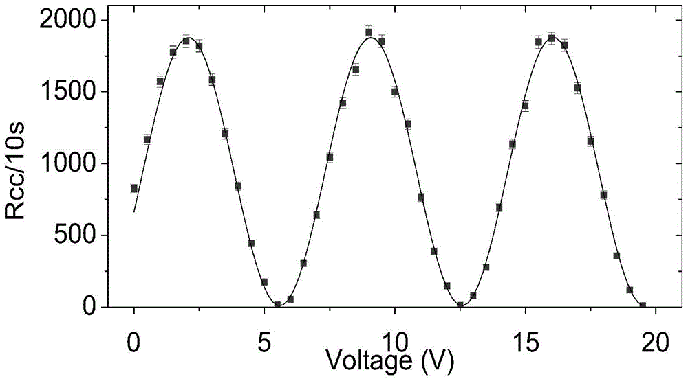
[0033] Example 1: The pump light is 780nm, and the degenerate photon pair is 1560nm. When the electrodes 8, 9, and 10 are set to 8mm, the voltage of 7V can cause the relative phase change of the two pumping lights by 2π, so that the output photon state of the chip goes through a complete change cycle from the focused state to the separated state and then to the focused state. image 3 It is a graph showing the variation of photon coincidence counts between the output optical fibers 26 and 27 with the applied voltage. The coincidence count in the figure changes periodically, the period is 7V, and the maximum and minimum values ​​represent the separated state and the bunched state, respectively. The first separation state corresponds to a voltage of 2.3V (theoretically should be 0V), which we call the offset voltage.

[0034] The design of the periodically polarized region 15 is as follows. Design its period to satisfy the quasi-phase-matching condition β for spontaneous param...


PUM


Abstract

A method for setting up a quantum light source chip based on an optical superlattice waveguide, which adopts the integration of a waveguide optical path, an optical superlattice, and an electro-optical modulator, and the waveguide optical path splits the incoming classical pumping laser beam through a waveguide beam splitter, splitting the beam After the laser light enters the optical superlattice region, the frequency is transferred to obtain entangled photon pairs, and then the entangled photon pairs continue to enter the interferometer for quantum interference; the phase of the interferometer is controlled by the built-in electro-optic modulator on the chip, and obtained through voltage adjustment. Several different quantum states.

Description

technical field [0001] The invention relates to the fields of quantum information technology, optoelectronic technology and nonlinear optics, in particular, a chip-based quantum light source is realized by using integrated optical technology and ideas. Background technique [0002] Entanglement is the core resource in quantum information technologies such as quantum communication and quantum computing. Therefore, how to prepare entangled light sources, especially adjustable, efficient, stable, and portable entangled light sources has always been a research difficulty and hot spot in the field of quantum information. The methods for generating entangled photon pairs historically include: (1) atomic cascade transitions [1]; (2) four-wave mixing processes in atomic systems [2]; (3) silicon-based [3,4] or optical fiber The four-wave mixing process of [5,6]; (4) the optical parametric down-conversion process in second-order nonlinear crystals [7,8]. Among them, the atomic casca...

Claims


Application Information

Patent Timeline
Patent Type & Authority Patents(China)
IPC IPC(8): G02F1/35
CPCG02F1/3558G02F1/21G02F1/3775G02B6/12033G02B6/12011G02B6/12014G02B6/12019G02B6/12016G02B2006/1204G02B2006/1215G02B2006/12159G02B2006/12142G02B2006/12152
Inventor 徐平金华祝世宁
Owner NANJING UNIV
Why Eureka
Try Eureka