
An electronically controlled polarization entangled state generation chip based on periodically poled lithium niobate waveguide

A periodic polarization, lithium niobate technology, applied in the fields of quantum information technology, optoelectronic technology and nonlinear optics, can solve problems such as large, unstable and complex optical paths

Active Publication Date: 2021-09-10
NANJING UNIV
View PDF5 Cites 0 Cited by
  • Summary
  • Abstract
  • Description
  • Claims
  • Application Information

AI Technical Summary

Problems solved by technology

The general polarization entanglement source is realized by the birefringence matching of bulk optical crystals [15], or the coexistence of dual phase matching in periodically polarized crystals [16]. Beamers[17], dichroic mirrors[18] and other optical components are used to assist the implementation, resulting in the optical path of entangled light sources being generally complex, bulky and unstable.
At the same time, the general disadvantage of existing solutions is that one optical path can only output one kind of polarization entanglement, such as one of the polarization entangled states. Bell-based designs have been reported, and quantum information processing often requires different polarization entangled states and fast switching of polarization entangled states
The above requirements prompt people to look for chip-like, dynamically switchable polarization entanglement generation methods, which cannot be realized by traditional implementation schemes.

Method used


Image

  • An electronically controlled polarization entangled state generation chip based on periodically poled lithium niobate waveguide
  • An electronically controlled polarization entangled state generation chip based on periodically poled lithium niobate waveguide
  • An electronically controlled polarization entangled state generation chip based on periodically poled lithium niobate waveguide

Examples


Embodiment 1

[0059] Polarization-entangled chip setup at 1550nm.

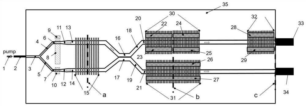
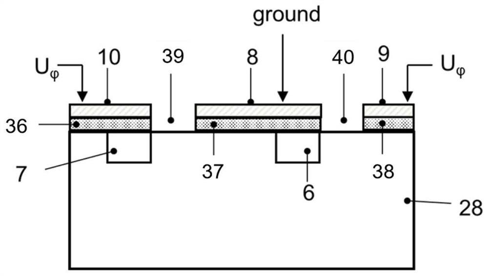
[0060] The pump light is 780nm, and the degenerate photon pair is 1560nm. When the length of the electrodes 8, 9, and 10 is set to 4.7 mm, the voltage of 11.0 volts can cause the relative phase of the two pump lasers to change by 2π.

[0061] The design of the periodically polarized region 15 is as follows. Design its period to satisfy the quasi-phase-matching condition β for spontaneous parametric downconversion in the waveguide p -β s -β i =2π / Λ, where β p ,β s ,β i are the fundamental mode propagation constants of the pump, signal and idler light respectively, which are jointly determined by the dispersion of the lithium niobate material and the waveguide processing technology. For the titanium diffusion waveguide, both horizontally polarized light and vertically polarized light can propagate, using the nonlinear coefficient d 31 . According to our process conditions, changing the polarization period will corres...

Embodiment 2

[0067] Example 2: Polarization-entangled chip setup around 800nm.

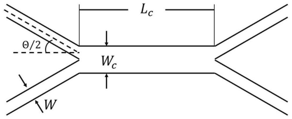
[0068] The polarization entanglement chip setup near 800nm ​​is very similar to that of 1550nm. Pumping with pump light near 400nm, the waveguide on the chip is changed to a single-mode waveguide of 400nm and 800nm, and the polarization period of the polarized area is correspondingly changed to The polarization period of the 400nm to 800nm ​​process is specified, and the other functional units are designed according to 800nm, but the polarization beam splitting needs to be designed separately, and the small-angle cross polarization beam splitting design is adopted. The simulation design results are given below. The design found that the width W of the incident waveguide is 7.5 microns, the included angle Θ is 1.49 degrees, and the width W of the waveguide in the coupling region c 15 µm, length L c to 6000 microns. Use Rsoft software to simulate such as Figure 12 , and the left and right pictures are the b...

Embodiment 3

[0069] Embodiment 3: Polarization entanglement chip for polarization beam splitting realized by composite process of proton exchange waveguide and titanium diffusion waveguide.

[0070] figure 1 In Region III, there are various on-chip ways to realize the polarization beam splitting function. For example, using the proton exchange waveguide and titanium diffusion waveguide composite technology to design a non-fully symmetrical three-waveguide coupling structure, such as Figure 13 . Waveguides 1 and 3 are titanium diffused lithium niobate waveguides, and waveguide 2 is a proton exchange waveguide. Waveguides 1 and 3 support horizontally and vertically polarized light, and waveguide 2 only supports vertically polarized light. Using this characteristic, a certain coupling length is set, the vertically polarized light is coupled to the cross output of the waveguide 3(1), and the horizontally polarized light is not coupled, thereby realizing polarization beam splitting. Wavegu...


PUM

PropertyMeasurementUnit
lengthaaaaaaaaaa
conversion efficiencyaaaaaaaaaa
refractive indexaaaaaaaaaa

Abstract

The electronically controlled polarization entangled state generation chip based on periodically polarized lithium niobate waveguide includes a pump beam splitting region, a periodically polarized region, a waveguide optical phase modulator, a waveguide optical path polarization beam splitter, and a dynamic electronically controlled photon delay device. constitute. The pump light beam splitting area is composed of a Y beam splitter and a phase modulator, which realizes the beam splitting and relative phase control of the pump light. The periodically polarized region is composed of periodically inverted ferroelectric domains on two separate waveguides, in which parametric down-conversion photon pairs based on second-order nonlinearity are realized respectively. The waveguide-based optical phase modulator is to make electrodes above the waveguide, and by applying an electric field to change the refractive index of the waveguide to control the phase of photons. The waveguide optical path polarization beam splitter realizes the separation of photons of different polarizations, and realizes the polarization beam splitting operation of the photon pairs generated in the two waveguides. The invention provides a chip-type, stable, high-brightness, high-entanglement, and dynamically switchable polarization entanglement output device.

Description

technical field [0001] The invention relates to the fields of quantum information technology, optoelectronic technology and nonlinear optics, in particular, a chip-based quantum light source is realized by using integrated optical technology and ideas. Background technique [0002] Entanglement is the core resource in quantum information technologies such as quantum communication and quantum computing. Therefore, how to prepare entangled light sources, especially adjustable, efficient, stable, and portable entangled light sources has always been a research difficulty and hot spot in the field of quantum information. The methods for generating entangled photon pairs historically include: (1) atomic cascade transitions [1]; (2) four-wave mixing processes in atomic systems [2]; (3) silicon-based [3,4] or optical fiber The four-wave mixing process of [5,6]; (4) the optical parametric down-conversion process in second-order nonlinear crystals [7,8]. Among them, the atomic casca...

Claims


Application Information

Patent Timeline
Patent Type & Authority Patents(China)
IPC IPC(8): G02F1/05G02F1/035G02F1/01G02B6/125G02B27/28G02B6/12G02F1/355G02F1/365
CPCG02B6/12G02B6/125G02B27/283G02B2006/12035G02B2006/1204G02B2006/12045G02F1/0136G02F1/0353G02F1/0508G02F1/3551G02F1/365
Inventor 徐平孙昌伟任坤乾龚彦晓谢臻达祝世宁
Owner NANJING UNIV
Learn More