Unit pixel, array substrate, display apparatus, and manufacture methods thereof
一种阵列基板、显示装置的技术,应用在半导体/固态器件制造、电气元件、半导体器件等方向,能够解决漏电流大等问题
- Summary
- Abstract
- Description
- Claims
- Application Information
AI Technical Summary
Problems solved by technology
Method used
Image

Examples
no. 1 example
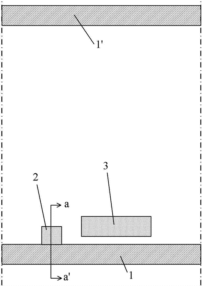
[0064] figure 2 It is a top view of a unit pixel of a first embodiment of the present invention after forming a gate line and a gate of a TFT. Such as figure 2 As shown, the obliquely shaded area is the grid line area 1 and 1', and the area surrounded by the grid line area and the dotted line is the area of a unit pixel. In this view, there are also gate regions 2 and 3 forming TFTs including region 2 of the gate switching TFT and region 3 of the data driving TFT.
[0065] In this embodiment, the material for forming the gate line in the above gate line region is a stacked layer structure, which respectively includes a first MoW layer, a Cu layer and a second MoW layer from bottom to top. And the gate electrode formed in the gate region of the TFT is composed of the first MoW layer.
[0066] exist figure 2 An active layer and source-drain electrode lines are then formed on the unit pixel shown, so as to complete the fabrication of the entire unit pixel. image 3 is a...
no. 2 example
[0082] The second embodiment also relates to a unit pixel structure of an array substrate of a display device and a manufacturing method thereof. The source-drain electrode line of the unit pixel adopts a MoW / Cu / MoW stack structure, while the source-drain electrode of the TFT uses a layer of MoW.
[0083] Figure 5It is a top view without forming source-drain electrode lines and source-drain electrodes of TFT in this embodiment. As shown in the figure, the gate line has been formed in the gate line area 4 and 4', and the gate area 5, 6 of the TFT forms the gate of the TFT, wherein the TFT gate area 5 is the gate switch TFT The area where the gate is located, the TFT gate area 6 is the area where the gate of the data-driven TFT is located.
[0084] In the present invention, the source-drain electrode lines include data lines and VDD lines. The data line is used to provide data driving, and the VDD line is used to provide a current source line for emitting light to the OLED. ...
PUM
 Abstract
Description
Claims
Application Information