Lamination type piezoresistor network and making method thereof

A varistor and chip technology, used in varistor, resistor manufacturing, resistors, etc., can solve the problems of unfavorable equipment miniaturization, low component installation efficiency, and large occupied area, so as to reduce the cost of the whole machine and improve the Installation density and efficiency, the effect of solving performance deterioration

Active Publication Date: 2010-01-06
SHENZHEN ZHENHUA FU ELECTRONICS +1
View PDF0 Cites 6 Cited by
  • Summary
  • Abstract
  • Description
  • Claims
  • Application Information

AI Technical Summary

Problems solved by technology

[0004] The traditional chip varistor is a single independent product. In terms of multi-line protection, it occupies a large area, which is not conducive to the miniaturization of equipment, and the installation efficiency of components is low, resulting in high cost of the whole machine

Method used


Image

  • Lamination type piezoresistor network and making method thereof
  • Lamination type piezoresistor network and making method thereof
  • Lamination type piezoresistor network and making method thereof

Examples


Embodiment Construction

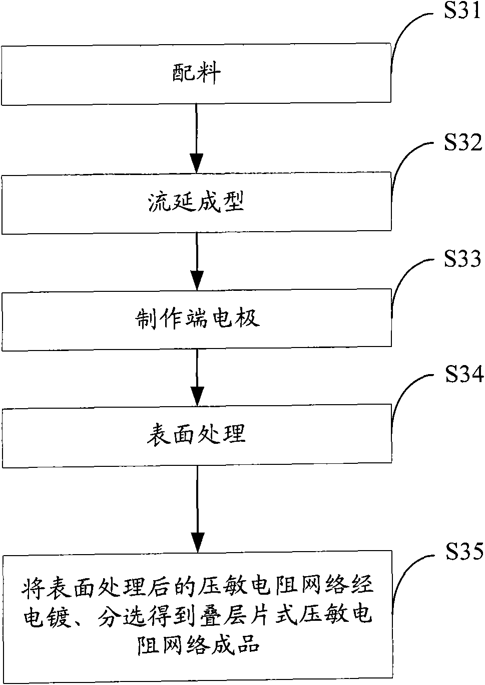
[0026] In order to make the object, technical solution and advantages of the present invention clearer, the present invention will be further described in detail below in conjunction with the accompanying drawings and embodiments. It should be understood that the specific embodiments described here are only used to explain the present invention, not to limit the present invention.

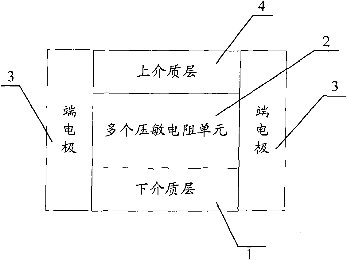
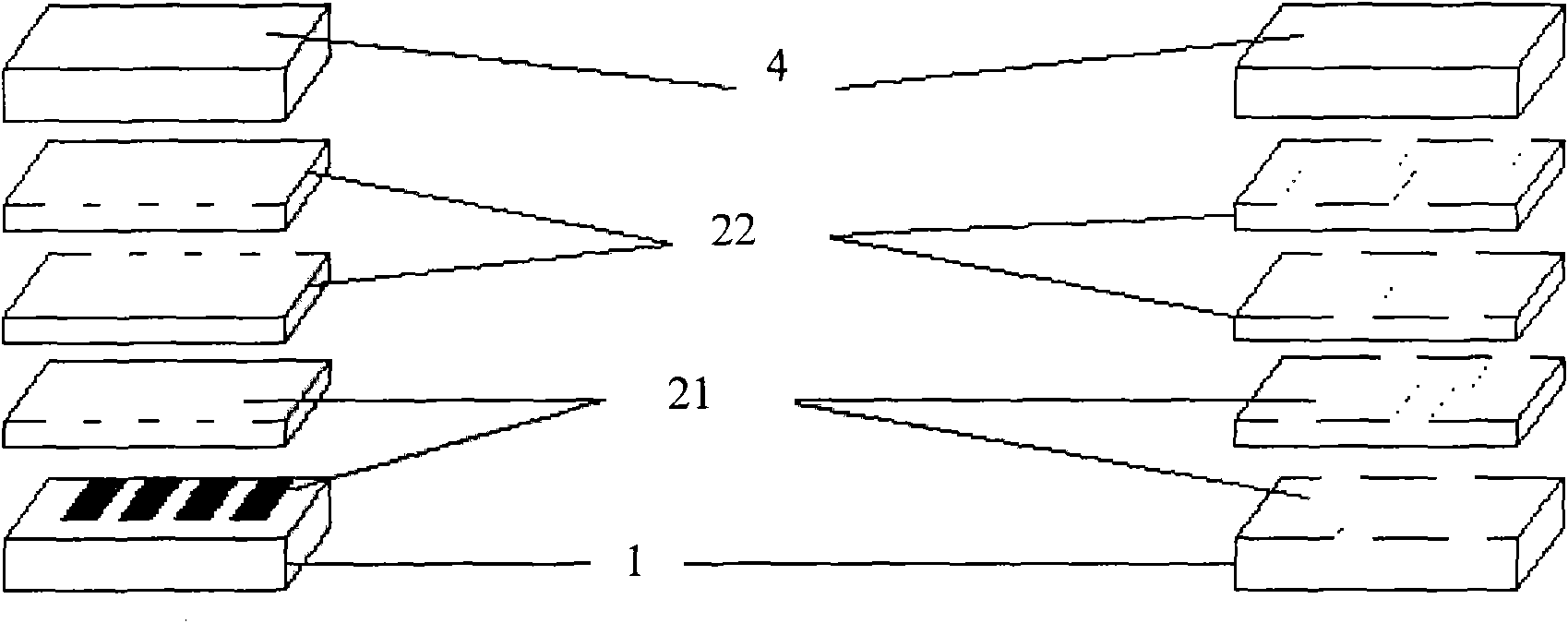
[0027] The multilayer chip varistor network provided by the embodiment of the present invention integrates a plurality of discrete varistor units, which is convenient to use in multi-line overvoltage protection, improves the component installation density and efficiency, and reduces the cost of the whole machine , to achieve miniaturization.

[0028] The multilayer chip varistor network provided by the embodiment of the present invention can be applied to the efficient installation of electronic equipment such as mobile communications, PDAs, and computers in multi-line overvoltage protection circui...


PUM


Abstract

The invention provides a lamination type piezoresistor network and a making method thereof, belonging to the field of electric elements. The lamination type piezoresistor network comprises a lower dielectric layer, a plurality of piezoresistor units, end electrodes and an upper dielectric layer, wherein the piezoresistor units are formed on the lower dielectric layer and mutually independent; the end electrodes are connected to both end parts of the piezoresistor units; the upper dielectric layer is combined with the lower dielectric layer attached by the piezoresistor units; and a piezoresistor further comprises an inner electrode attached on the lower dielectric layer and a piezoresistor film covered on the inner electrode. The lamination type piezoresistor network integrates the independent piezoresistor units into a whole, is convenient to use on the aspect of multiline overvoltage protection, enhances the installation density and the installation efficiency of the elements, reduces the integral machine cost and realizes the miniaturization.

Description

technical field [0001] The invention belongs to the field of electronic components, in particular to a laminated chip varistor network and a manufacturing method thereof. Background technique [0002] Transient voltage, surge voltage and electrostatic discharge (Electro-Static Discharge, ESD) damage to integrated circuits and semiconductor devices are well known, that is, semiconductor devices are very sensitive to voltage and current surges, even if 10 -6 The magnitude of electrostatic noise may also cause damage or failure of components and circuits. In recent years, the low-voltage development trend of integrated circuits and semiconductor devices is obvious, especially the development of low-voltage handheld electronic products makes overvoltage protection components more and more important, so suppress transient voltage, surge voltage and ESD chip components are undoubtedly indispensable. [0003] With the continuous miniaturization of mobile communication, personal d...

Claims


Application Information

Patent Timeline
Patent Type & Authority Applications(China)
IPC IPC(8): H01C7/10H01C17/00H01C17/28H01C17/30
Inventor 徐鹏飞丁晓鸿付贤民马建华黄波黄寒寒徐平友尚晓云段凛
Owner SHENZHEN ZHENHUA FU ELECTRONICS
Why Eureka
Try Eureka