Method for preparing ultra-shallow junction on surface of semiconductor chip through laser

A semiconductor, N-type semiconductor technology, applied in semiconductor/solid-state device manufacturing, electrical components, circuits, etc., can solve the problems of doping lateral and vertical diffusion, PN junction size limitations, complex processes, etc., to simplify the process, save Annealing process, the effect of shortening the process time

Inactive Publication Date: 2010-06-02
GD SOLAR +2
View PDF1 Cites 6 Cited by
  • Summary
  • Abstract
  • Description
  • Claims
  • Application Information

AI Technical Summary

Problems solved by technology

This processing method is not only complicated in process and high in cost, but most importantly, it will cause lateral and vertical diffusion of doping during the processing of doping, which limits the size of PN junction.

Method used


Image

  • Method for preparing ultra-shallow junction on surface of semiconductor chip through laser
  • Method for preparing ultra-shallow junction on surface of semiconductor chip through laser

Examples


Embodiment 1

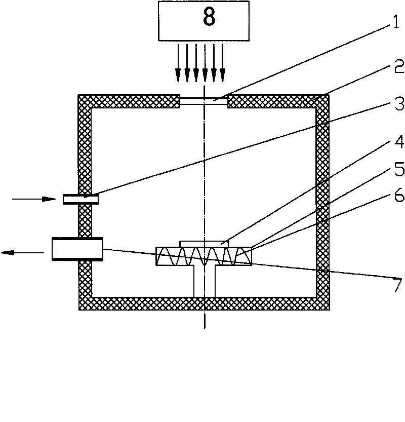
[0030] Using the N-type single crystal silicon of 156mm×156mm×180 μm as the substrate, the present invention is used to perform doping on the N-type semiconductor substrate to form an ultra-shallow junction, so as to further illustrate the present invention. The process steps are as follows: 1. Put the cleaned N-type silicon wafer on the slide table in the vacuum chamber, and the silicon wafer is facing the transparent glass window 1. 2. Close the vacuum chamber door, and evacuate the vacuum chamber to 3.0 ×10 -3 Pa, turn on the heater at the same time to heat the substrate, the heating temperature is 350°C. 3. When the vacuum degree reaches the background vacuum degree, the heating temperature is stabilized at 350°C for more than 10 minutes, and after the silicon wafer is evenly heated, the flow rate of 500 sccm is passed into the vacuum chamber. 2 h 6 and H 2 The mixed gas, where B 2 h 6 The percentage content is 5%. At the same time, adjust the pumping rate to keep th...

Embodiment 2

[0032] Using the P-type single crystal silicon of 156mm×156mm×180 μm as the substrate, the present invention is used to perform doping on the P-type semiconductor substrate to form an ultra-shallow junction, so as to further illustrate the present invention. The process steps are as follows: 1. Put the cleaned P-type silicon wafer on the slide table in the vacuum chamber, and the silicon wafer is facing the transparent glass window 1. 2. Close the door of the vacuum chamber, and evacuate the vacuum chamber to 10Pa , and at the same time turn on the heater to heat the substrate at a heating temperature of 400°C. 3. When the vacuum degree reaches the background vacuum degree, the heating temperature is stable at 400°C for more than 15 minutes, and after the silicon wafer is evenly heated, a PH with a flow rate of 300 sccm is introduced into the vacuum chamber. 3 and H 2 The mixed gas, where PH 3The percentage content is 8%. At the same time, adjust the pumping rate to keep th...


PUM


Abstract

The invention discloses a method for preparing an ultra-shallow junction on the surface of a semiconductor chip through laser, which comprises the following steps of: leading the mixture of H2 and another gas at the speed with the lead-in gas flow capacity of 50-1000sccm under a vacuum condition, and doping the mixed gas onto the surface of the semiconductor chip when chip lattices are activated; using laser to irradiate the semiconductor chip to instantly increase the temperature of the semiconductor chip by 1000-1400DEG C, and finally forming the ultra-shallow junction on the surface of the semiconductor chip, further preferably, the instant increased temperature of the chip is 1200DEG C. The depth of the prepared ultra-shallow junction can be smaller than 30 nanometers, and the doping concentration can be adjusted according to specific requirements. The invention simplifies working procedures and shortens process time. Gas elements can be adjusted, being beneficial to adjusting the doping concentration according to the different purposes of the ultra-shallow junction. The lead-in gas flow capacity is controlled, being beneficial to forming a uniform atmosphere in a vacuum chamber and ensuring the uniformity of the prepared ultra-shallow junction.

Description

technical field [0001] The invention relates to the technical field of semiconductor preparation of PN junctions, in particular to a method for preparing ultra-shallow junctions on the surface of semiconductor substrates by laser. Background technique [0002] With the miniaturization of semiconductor devices, the technical requirements for the preparation of PN junctions are also getting higher and higher, and it is required to prepare high-quality ultra-shallow junctions with smaller and smaller lateral dimensions and depths. Various methods for preparing ultra-shallow junctions in the prior art are formed by doping in various ways and then annealing at a certain temperature. For example, the patent application No. 01806216.4 "Method for forming ultra-shallow junction by laser annealing and rapid heating annealing" discloses an annealing process for the second half of the preparation of ultra-shallow junction. First, the substrate is irradiated with laser light sufficient ...

Claims


Application Information

Patent Timeline
Patent Type & Authority Applications(China)
IPC IPC(8): H01L21/18H01L21/268
Inventor 张宏勇刘莹郑振生
Owner GD SOLAR
Why Eureka
Try Eureka